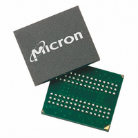
MT48LC4M32B2B5-7:G Micron Technology Inc, MT48LC4M32B2B5-7:G Datasheet - Page 45

MT48LC4M32B2B5-7:G
Manufacturer Part Number
MT48LC4M32B2B5-7:G
Description
DRAM Chip SDRAM 128M-Bit 4Mx32 3.3V 90-Pin VFBGA Tray
Manufacturer
Micron Technology Inc
Type
SDRAMr
Datasheet
1.MT48LC4M32B2P-7G_TR.pdf
(67 pages)
Specifications of MT48LC4M32B2B5-7:G
Density
128 Mb
Maximum Clock Rate
143 MHz
Package
90VFBGA
Address Bus Width
14 Bit
Operating Supply Voltage
3.3 V
Maximum Random Access Time
17|8|5.5 ns
Operating Temperature
0 to 70 °C
Format - Memory
RAM
Memory Type
SDRAM
Memory Size
128M (4Mx32)
Speed
143MHz
Interface
Parallel
Voltage - Supply
3 V ~ 3.6 V
Package / Case
90-VFBGA
Organization
4Mx32
Address Bus
14b
Access Time (max)
17/8/5.5ns
Operating Supply Voltage (typ)
3.3V
Package Type
VFBGA
Operating Temp Range
0C to 70C
Operating Supply Voltage (max)
3.6V
Operating Supply Voltage (min)
3V
Supply Current
175mA
Pin Count
90
Mounting
Surface Mount
Operating Temperature Classification
Commercial
Lead Free Status / RoHS Status
Lead free / RoHS Compliant
Lead Free Status / RoHS Status
Compliant, Lead free / RoHS Compliant
Available stocks
Company
Part Number
Manufacturer
Quantity
Price
Company:
Part Number:
MT48LC4M32B2B5-7:G
Manufacturer:
Micron Technology Inc
Quantity:
10 000
Company:
Part Number:
MT48LC4M32B2B5-7:G TR
Manufacturer:
Micron Technology Inc
Quantity:
10 000
Table 15:
Table 16:
Table 17:
PDF: 09005aef80872800/Source: 09005aef80863355
128MbSDRAMx32_2.fm - Rev. L 1/09 EN
Parameter/Condition
Parameter/Condition
Parameter
Supply voltage
Input high voltage: Logic 1; All inputs
Input low voltage: Logic 0; All inputs
Input leakage current:
Any input 0V ≤ V
Output leakage current:
DQs are disabled; 0V ≤ V
Output levels:
)Output high voltage (I
Output low voltage (I
Operating current: Active mode;
Burst = 2; READ or WRITE;
Standby current: Power-Down mode;
CKE = LOW; All banks idle
Standby current: Active mode; CS# = HIGH;
CKE = HIGH; All banks active after
No accesses in progress
Operating current: Burst mode; Continuous burst;
READ or WRITE; All banks active, CL = 3
Auto refresh current:
CL = 3; CKE, CS# = HIGH
Self refresh current: CKE ≤ 0.2V
Input Capacitance: CLK
Input Capacitance: All other input-only pins
Input/Output Capacitance: DQs
DC Electrical Characteristics and Operating Conditions
Notes 1, 6 apply to the entire table; notes appear on page 48; V
I
Notes 1, 6, 11, 13 apply to the entire table; notes appear on page 48; V
Capacitance
Note 2 applies to the entire table; notes appear on page 48
DD
IN
Specifications and Conditions
≤ V
OUT
DD
OUT
OUT
(All other pins not under test = 0V)
= 4mA)
t
RC =
= –4mA)
≤ V
DD
t
RC (MIN); CL = 3
Q
t
RCD met;
t
RFC =
t
RFC (MIN)
45
V
Symbol
Symbol
DD
I
I
I
I
I
I
V
V
V
DD
DD
DD
DD
DD
DD
, V
I
Vil
Symbol
OZ
OH
I
OL
IH
I
Micron Technology, Inc., reserves the right to change products or specifications without notice.
1
2
3
4
5
6
DD
C
C
C
I
I
I
1
2
o
Q
DD
Min
= +3.3V ±0.3V, V
–0.3
190
195
320
2.4
–5
–5
65
-6
3
2
2
2
–
DD
Min
2.5
2.5
4.0
Max
, V
Electrical Specifications
V
DD
DD
Max
Q = +3.3V ±0.3V
165
175
320
3.6
0.8
0.4
55
-7
5
5
–
2
2
+ 0.3
©2001 Micron Technology, Inc. All rights reserved.
128Mb: x32 SDRAM
DD
Max
Q = +3.3V ±0.3V
4.0
4.0
6.5
Units
Units
mA
mA
mA
mA
mA
mA
µA
µA
V
V
V
V
V
3, 18, 19,
3, 18, 19,
3, 12, 18,
Units
Notes
Notes
19, 26
19, 26
pF
pF
pF
22
22
26
26
4


