ZY8140G-R1 POWER ONE, ZY8140G-R1 Datasheet - Page 15
ZY8140G-R1
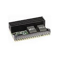
Manufacturer Part Number
ZY8140G-R1
Description
Module DC-DC 1-OUT 0.5V to 5.5V 40A 17-Pin SIP
Manufacturer
POWER ONE
Type
Step Downr
Datasheet
1.ZY8140G.pdf
(30 pages)
Specifications of ZY8140G-R1
Number Of Outputs
1
Output Voltage
0.5 to 5.5 V
Package
17SIP
Output Current
40 A
Input Voltage
8 to 14 V
Switching Regulator
Yes
Output Power
220 W
Input Voltage Range
8 V to 14 V
Output Voltage (channel 1)
0.5 V to 5.5 V
Output Current (channel 1)
40 A
Package / Case Size
SIP
Package / Case
SIP
Product
Non-Isolated / POL
Lead Free Status / Rohs Status
Lead free / RoHS Compliant


8.1.1
The output voltage programming range is from 0.5V
to 3.65V. To improve the resolution of the output
voltage settings, the voltage range is divided into
sub-ranges as shown in Table 2.
8.1.2
If the output voltage needs to be varied by a certain
percentage, the margining function can be utilized.
The margining can be programmed in the GUI
Output Configuration window or directly via the I
bus using high level commands as described in the
‘”DPM Programming Manual”.
In order to properly margin POLs that are connected
in parallel, the POLs must be members of one of the
Parallel Buses.
Configuration Window shown in Figure 45.
8.1.3
Optimal voltage positioning increases the voltage
regulation window by properly positioning the output
voltage setpoint. Positioning is determined by the
load regulation that can be programmed in the GUI
Output Configuration window shown in Figure 17 or
directly via the I
register shown in Figure 28.
Figure 19 illustrates optimal voltage positioning
concept. If no load regulation is programmed, the
headroom (voltage differential between the output
voltage
approximately half of the voltage regulation window.
When load regulation is programmed, the output
voltage
increases, so the VI characteristic will have a
negative slope. Therefore, by properly selecting the
operating point, it is possible to increase the
headroom as shown in the picture.
ZD-01977 Rev. 1.1, 01-Jul-10
V
OUT MIN
Table 2. Output Voltage Adjustment Resolution
0.500
2.025
will
Output Voltage Setpoint
Output Voltage Margining
Optimal Voltage Positioning
setpoint
, V
decrease
2
C bus by writing into the CLS
and
V
Refer to the
OUT MAX
2.000
2.75
as
a
, V
regulation
the
output
Resolution, mV
GUI System
www.power-one.com
12.5
25
limit)
current
2
C
is
8V to 14V Input
Increased headroom allows tolerating larger voltage
deviations. For example, the step load change from
light to heavy load will cause the output voltage to
drop. If the optimal voltage positioning is utilized, the
output voltage will stay within the regulation window.
Otherwise, the output voltage will drop below the
lower regulation limit. To compensate for the voltage
drop external output capacitance will need to be
added, thus increasing cost and complexity of the
system.
The effect of optimal voltage positioning is shown in
Figure 20 and Figure 21.
output load causes large peak-to-peak deviation of
the output voltage. By programming load regulation,
the peak to peak deviation is dramatically reduced.
Figure 20. Transient Response without Optimal Voltage
Upper Regulation
Lower Regulation
ZY8140 40A DC-DC Intelligent POL
Limit
Limit
Figure 19. Concept of Optimal Voltage Positioning
V
OUT
Positioning
Load Regulation
Headroom with
Light
Load
Headroom without
Load Regulation
0.5V to 3.65V Output
Operating
I
OUT
Point
In this case, switching
Load Regulation
VI Curve With
Page 15 of 30
Data Sheet
VI Curve Without
Load Regulation
Heavy
Load
Related parts for ZY8140G-R1
Image
Part Number
Description
Manufacturer
Datasheet
Request
R

Part Number:
Description:
PROGBL CONVERT DC-DC 40A OUT SMD
Manufacturer:
POWER ONE
Datasheet:

Part Number:
Description:
Zy8140 40a Dc-dc Intelligent Pol
Manufacturer:
Power-One
Datasheet:

Part Number:
Description:
SWITCHING POWER SUPPLIES, SINGLE OUTPUT, 80 WATTS
Manufacturer:
POWER ONE
Datasheet:
Part Number:
Description:
HAS SERIES - 30 WATT
Manufacturer:
POWER ONE
Datasheet:
Part Number:
Description:
SINGLE OUTPUT
Manufacturer:
POWER ONE
Datasheet:
Part Number:
Description:
BRS DC/DC converters(1.5 WATT)
Manufacturer:
Power-One
Datasheet:
Part Number:
Description:
3...15 Watt DC-DC Converter
Manufacturer:
Power-One
Datasheet:
Part Number:
Description:
HBS SERIES - 100 WATT
Manufacturer:
Power-One
Datasheet:
Part Number:
Description:
3...15 Watt DC-DC Converter
Manufacturer:
Power-One
Datasheet:
Part Number:
Description:
BUS DC/DC converters(3 WATT)
Manufacturer:
Power-One
Datasheet:
Part Number:
Description:
HES SERIES 150 WATT
Manufacturer:
Power-One
Datasheet: