ZY8140G-R1 POWER ONE, ZY8140G-R1 Datasheet - Page 18
ZY8140G-R1
Manufacturer Part Number
ZY8140G-R1
Description
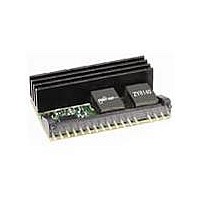
Module DC-DC 1-OUT 0.5V to 5.5V 40A 17-Pin SIP
Manufacturer
POWER ONE
Type
Step Downr
Datasheet
1.ZY8140G.pdf
(30 pages)
Specifications of ZY8140G-R1
Number Of Outputs
1
Output Voltage
0.5 to 5.5 V
Package
17SIP
Output Current
40 A
Input Voltage
8 to 14 V
Switching Regulator
Yes
Output Power
220 W
Input Voltage Range
8 V to 14 V
Output Voltage (channel 1)
0.5 V to 5.5 V
Output Current (channel 1)
40 A
Package / Case Size
SIP
Package / Case
SIP
Product
Non-Isolated / POL
Lead Free Status / Rohs Status
Lead free / RoHS Compliant


Note
protection thresholds and Power Good limits are
defined as percentages of the output voltage.
Therefore, the absolute levels of the thresholds
change when the output voltage setpoint is changed
either by output voltage adjustment or by margining.
In addition, a user can change type of protections
(latching
protections. These settings are programmed in the
GUI Fault Management window shown in Figure 30
or directly via the I
shown in Figure 31.
ZD-01977 Rev. 1.1, 01-Jul-10
Bit 7:5 LR[2:0], Load regulation configuration
Bit 4
Bit 3:0 CLS[3:0], Current limit setting
Bit 7:5 Unimplemented , read as ‘0’
Bit 4
Bit 3:2 OVPL[1:0] : Set Over Voltage Protection
Bit 1:0 UVPL[1:0] : Set Under Voltage Protection Level
R/W-0
LR2
Bit 7
Bit 7
---
U
Figure 29. Protection Configuration Register PC2
Figure 28. Current Limit Setpoint Register CLS
000: 0 V/A/Ohm
001: 0.39 V/A/Ohm
010: 0.78 V/A/Ohm
011: 1.18 V/A/Ohm
100: 1.57 V/A/Ohm
101: 1.96 V/A/Ohm
110: 2.35 V/A/Ohm
111: 2.75 V/A/Ohm
TCE, Temperature compensation enable
0: disabled
1: enabled
0h: corresponds to 37%
1h: corresponds to 47%
…
Bh: corresponds to 140%
Values higher than Bh are translated to Bh (140%)
PGLL: Set Power Good Low Level
1 = 95% of Vo
Level
00 = 110% of Vo
01 = 120% of Vo
10 = 130% of Vo (Default)
00 = 75% of Vo (Default)
01 = 80% of Vo
10 = 85% of Vo
that
0 = 90% of Vo (Default)
11 = 130% of Vo
11 = 90% of Vo
R/W-0
LR1
---
or
U
the
non-latching)
R/W-0
LR0
---
U
2
overvoltage
C by writing into the PC1 register
R/W-1
R/W-0
PGLL
TCE
OVPL1
R/W-1
R/W-1
CLS3
or
and
OVPL0
R/W-0
R/W-0
CLS2
R = Readable bit
W = Writable bit
U = Unimplemented bit,
- n = Value at POR reset
R = Readable bit
W = Writable bit
U = Unimplemented bit,
- n = Value at POR reset
disable
read as ‘0’
read as ‘0’
www.power-one.com
undervoltage
UVPL1
R/W-1
R/W-0
CLS1
certain
UVPL0
R/W-1
R/W-0
CLS0
Bit 0
Bit 0
8V to 14V Input
If the non-latching protection is selected, a POL will
attempt to restart every 130ms until the condition
that triggered the protection is removed.
restarting, the output voltages follow tracking and
sequencing settings.
If the latching type is selected, a POL will turn off and
stay off. The POL can be turned on after 130ms, if
the condition that caused the fault is removed and
the respective bit in the ST register was cleared, or
the Turn On command was recycled, or the input
voltage was recycled.
ZY8140 40A DC-DC Intelligent POL
Bit 7
Bit 6
Bit 5
Bit 4
Bit 3
Bit 2
Bit 1
Bit 0
R/W-0
TRE
Bit 7
Figure 31. Protection Configuration Register PC1
TRE: Tracking fault enable
1 = enabled
0 = disabled
PVE: Phase voltage error enable
1 = enabled
0 = disabled
TRP: Tracking fault protection
1 = latching
0 = non latching
OTP: Overtemperature protection configuration
1 = latching
0 = non latching
OCP: Overcurrent protection configuration
1 = latching
0 = non latching
UVP: Undervoltage protection configuration
1 = latching
0 = non latching
OVP: Overvoltage protection configuration
1 = latching
0 = non latching
PVP: Phase Voltage Protection (Not Active)
1 = latching
0 = non latching
R/W-1
Figure 30. Fault Management Window
PVE
R/W-0
TRP
0.5V to 3.65V Output
R/W-0
OTP
R/W-0
OCP
Page 18 of 30
R/W-0
UVP
R = Readable bit
W = Writable bit
U = Unimplemented bit,
- n = Value at POR reset
Data Sheet
read as ‘0’
R/W-1
OVP
When
R/W-1
PVP
Bit 0
Related parts for ZY8140G-R1
Image
Part Number
Description
Manufacturer
Datasheet
Request
R

Part Number:
Description:
PROGBL CONVERT DC-DC 40A OUT SMD
Manufacturer:
POWER ONE
Datasheet:

Part Number:
Description:
Zy8140 40a Dc-dc Intelligent Pol
Manufacturer:
Power-One
Datasheet:

Part Number:
Description:
SWITCHING POWER SUPPLIES, SINGLE OUTPUT, 80 WATTS
Manufacturer:
POWER ONE
Datasheet:
Part Number:
Description:
HAS SERIES - 30 WATT
Manufacturer:
POWER ONE
Datasheet:
Part Number:
Description:
SINGLE OUTPUT
Manufacturer:
POWER ONE
Datasheet:
Part Number:
Description:
BRS DC/DC converters(1.5 WATT)
Manufacturer:
Power-One
Datasheet:
Part Number:
Description:
3...15 Watt DC-DC Converter
Manufacturer:
Power-One
Datasheet:
Part Number:
Description:
HBS SERIES - 100 WATT
Manufacturer:
Power-One
Datasheet:
Part Number:
Description:
3...15 Watt DC-DC Converter
Manufacturer:
Power-One
Datasheet:
Part Number:
Description:
BUS DC/DC converters(3 WATT)
Manufacturer:
Power-One
Datasheet:
Part Number:
Description:
HES SERIES 150 WATT
Manufacturer:
Power-One
Datasheet: