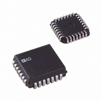
AD1671JP Analog Devices Inc, AD1671JP Datasheet - Page 3

AD1671JP
Manufacturer Part Number
AD1671JP
Description
ADC Single Pipelined 1.25MSPS 12-Bit Parallel 28-Pin PLCC
Manufacturer
Analog Devices Inc
Datasheet
1.AD1671JP.pdf
(16 pages)
Specifications of AD1671JP
Package
28PLCC
Resolution
12 Bit
Sampling Rate
1250 KSPS
Architecture
Pipelined
Number Of Analog Inputs
1
Digital Interface Type
Parallel
Input Type
Voltage
Polarity Of Input Voltage
Unipolar|Bipolar
Rohs Status
RoHS non-compliant
Number Of Bits
12
Sampling Rate (per Second)
1.25M
Data Interface
Parallel
Number Of Converters
2
Power Dissipation (max)
750mW
Voltage Supply Source
Analog and Digital, Dual ±
Operating Temperature
0°C ~ 70°C
Mounting Type
Surface Mount
Package / Case
28-LCC (J-Lead)
Lead Free Status / RoHS Status
Available stocks
Company
Part Number
Manufacturer
Quantity
Price
Part Number:
AD1671JP
Manufacturer:
ADI/亚德诺
Quantity:
20 000
Company:
Part Number:
AD1671JPZ
Manufacturer:
AD
Quantity:
1 000
REV. B
AC SPECIFICATIONS
Parameter
SIGNAL-TO-NOISE PLUS DISTORTION RATIO
EFFECTIVE NUMBER OF BITS (ENOB)
TOTAL HARMONIC DISTORTION (THD)
PEAK SPURIOUS OR PEAK HARMONIC COMPONENT
SMALL SIGNAL BANDWIDTH
FULL POWER BANDWIDTH
INTERMODULATION DISTORTION (IMD)
NOTES
1
2
Specifications subject to change without notice.
SWITCHING SPECIFICATIONS
Parameters
Conversion Time
Sample Rate
ENCODE Pulse Width High (Figure 1a)
ENCODE Pulse Width Low (Figure 1b)
DAV Pulse Width
ENCODE Falling Edge Delay
Start New Conversion Delay
Data and OTR Delay from DAV Falling Edge
Data and OTR Valid before DAV Rising Edge
NOTES
1
2
Specifications subject to change without notice.
f
f
indicated.
t
t
IN
A
DD
SS
(S/N + D)
2nd Order Products
3rd Order Products
= 99 kHz, f
amplitude = –0.5 dB (9.44 V p-p) bipolar mode full scale unless otherwise indicated. All measurements referred to a 0 dB ( 5 V) input signal, unless otherwise
is measured from when the outputs cross 0.4 V or 2.4 V to when the rising edge of DAV crosses 2.4 V with a 25 pF load capacitor on each output pin.
is measured from when the falling edge of DAV crosses 0.8 V to when the output crosses 0.4 V or 2.4 V with a 25 pF load capacitor on each output pin.
–0.5 dB Input
–20 dB Input
MSB, OTR
ENCODE
BIT 1–12
DAV
B
= 100 kHz with f
Figure 1a. Encode Pulse HIGH
t
ENC
DATA 0 (PREVIOUS)
SAMPLE
(T
f
lNPUT
= 1 MSPS.
MIN
t
to T
= 1OO kHz, unless otherwise noted)
C
MAX
with V
t
DD
(For all grades T
V
EE
t
DAV
= –5 V
CC
2
DATA 1
t
SS
= +5 V
t
R
5%; V
MIN
5%, V
Symbol
t
F
t
t
t
t
t
t
t
C
ENC
ENCL
DAV
F
R
DD
SS
S
2
to T
IL
1
–3–
= 0.8 V, V
LOGIC
MAX
1
with V
= +5 V
Min
68
11.2
MSB, OTR
IH
AD1671J/A/S
ENCODE
BIT 1–12
CC
= 2.0 V, V
= +5 V
DAV
Typ
70
50
–80
12
2
–80
–80
–85
10%, V
Min
20
20
150
0
0
20
20
Figure 1b. Encode Pulse LOW
OL
Max
–77
–75
–75
EE
–75
= 0.4 V and V
5%, V
= –5 V
DATA 0 (PREVIOUS)
LO61C
Typ
75
75
Min
68
11.2
= +5 V
5%, f
OH
= 2.4 V)
AD1671K
t
C
SAMPLE
Typ
71
51
–83
–81
12
2
–80
–85
10%,
= 1 MSPS,
t
DD
Max
800
1.25
50
300
t
DAV
Max
–77
–75
–75
–75
t
t
F
ENCL
t
SS
DATA 1
AD1671
t
R
Units
ns
MSPS
ns
ns
ns
ns
ns
ns
ns
Units
dB
dB
Bits
dB
MHz
MHz
dB
dB
dB


