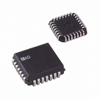
AD1671JP Analog Devices Inc, AD1671JP Datasheet - Page 7

AD1671JP
Manufacturer Part Number
AD1671JP
Description
ADC Single Pipelined 1.25MSPS 12-Bit Parallel 28-Pin PLCC
Manufacturer
Analog Devices Inc
Datasheet
1.AD1671JP.pdf
(16 pages)
Specifications of AD1671JP
Package
28PLCC
Resolution
12 Bit
Sampling Rate
1250 KSPS
Architecture
Pipelined
Number Of Analog Inputs
1
Digital Interface Type
Parallel
Input Type
Voltage
Polarity Of Input Voltage
Unipolar|Bipolar
Rohs Status
RoHS non-compliant
Number Of Bits
12
Sampling Rate (per Second)
1.25M
Data Interface
Parallel
Number Of Converters
2
Power Dissipation (max)
750mW
Voltage Supply Source
Analog and Digital, Dual ±
Operating Temperature
0°C ~ 70°C
Mounting Type
Surface Mount
Package / Case
28-LCC (J-Lead)
Lead Free Status / RoHS Status
Available stocks
Company
Part Number
Manufacturer
Quantity
Price
Part Number:
AD1671JP
Manufacturer:
ADI/亚德诺
Quantity:
20 000
Company:
Part Number:
AD1671JPZ
Manufacturer:
AD
Quantity:
1 000
REV. B
THEORY OF OPERATION
The AD1671 uses a successive subranging architecture. The
analog-to-digital conversion takes place in four independent
steps or flashes. The sampled analog input signal is subranged
to an intermediate residue voltage for the final 12-bit result by
utilizing multiple flashes with subtraction DACs (see the AD1671
functional block diagram).
The AD1671 can be configured to operate with unipolar (0 V to
+5 V, 0 V to +2.5 V) or bipolar ( 5 V, 2.5 V) inputs by con-
necting AIN (Pins 22, 23), SHA OUT (Pin 25) and BPO/UPO
(Pin 26) as shown in Figure 2.
The AD1671 conversion cycle begins by simply providing an
active HIGH level on the ENCODE pin (Pin 17). The rising
edge of the ENCODE pulse starts the conversion. The falling
edge of the ENCODE pulse is specified to operate within a win-
dow of time, less than 50 ns after the rising edge of ENCODE
or after the falling edge of DAV. The time window prevents
digitally coupled noise from being introduced during the final
stages of conversion. An internal timing generator circuit accu-
rately controls SHA, flash and DAC timing.
Upon receipt of an ENCODE command the input voltage is
held by the front-end SHA and the first 3-bit flash converts the
analog input voltage. The 3-bit result is passed to a correction
logic register and a segmented current output DAC. The DAC
output is connected through a resistor (within the Range/Span
Select Block) to SHA OUT. A residue voltage is created by sub-
tracting the DAC output from SHA OUT, which is less than
one eighth of the full-scale analog input. The second flash has
+2.5V
a. 0 V to +2.5V Input Range
+5V
TO
TO
c. 0 V to +5 V Input Range
0
0
Figure 2. AD1671 Input Range Connections
AIN2
AIN1
AIN1
AIN2
SHA OUT
BPO/UPO
REF IN
REF OUT
SHA OUT
BPO/UPO
REF IN
REF OUT
5k
5k
5k
5k
AD1671
AD1671
SHA
SHA
–2.5V
+2.5V
5V
TO
b. 2.5 V Input Range
d. 5 V Input Range
AIN1
AIN2
AIN1
AIN2
SHA OUT
BPO/UPO
REF IN
REF OUT
SHA OUT
BPO/UPO
REF IN
REF OUT
5k
5k
5k
5k
AD1671
AD1671
SHA
SHA
–7–
an input range that is configured with one bit of overlap with the
previous DAC. The overlap allows for errors during the flash
conversion. The first residue voltage is connected to the second
3-bit flash and to the noninverting input of a high speed, differ-
ential, gain of eight amplifier. The second flash result is passed
to the correction logic register and to the second segmented cur-
rent output DAC. The output of the second DAC is connected
to the inverting input of the differential amplifier. The differen-
tial amplifier output is connected to a two-step, backend, 8-bit
flash. This 8-bit flash consists of coarse and fine flash convert-
ers. The result of the coarse 4-bit flash converter, also config-
ured to overlap one bit of DAC 2, is connected to the correction
logic register and selects one of 16 resistors from which the fine
4-bit flash will establish its span voltage. The fine 4-bit flash is
connected directly to the output latches.
The internal timing generator automatically places the SHA into
the acquire mode when DAV goes LOW. Upon completion of
conversion (when DAV is set HIGH), the SHA has acquired the
analog input to the specified level of accuracy and will remain in
the sample mode until the next ENCODE command.
The AD1671 will flag an out-of-range condition when the input
voltage exceeds the analog input range. OTR (Pin 15) is active
HIGH when an out-of-range high or low condition exists. Bits
1–12 are HIGH when the analog input voltage is greater than
the selected input range and LOW when the analog input is less
than the selected input range.
AD1671 DYNAMIC PERFORMANCE
The AD1671 is specified for dc and dynamic performance. A
sampling converter’s dynamic performance reflects both quan-
tizer and sample-and-hold amplifier (SHA) performance. Quan-
tizer nonlinearities, such as INL and DNL, can degrade dynamic
performance. However, a SHA is the critical element which has to
accurately sample fast slewing analog input signals. The AD1671’s
high performance, low noise, patented on-chip SHA minimizes
distortion and noise specifications. Nonlinearities are minimized
by using a fast slewing, low noise architecture and subregulation
of the sampling switch to provide constant offsets (therefore
reducing input signal dependent nonlinearities).
Figure 3 is a typical 2k point Fast Fourier Transform (FFT)
plot of a 100 kHz input signal sampled at 1 MHz. The funda-
mental amplitude is set at –0.5 dB to avoid input signal clipping
of offset or gain errors. Note the total harmonic distortion is ap-
proximately –81 dB, signal to noise plus distortion is 71 dB and
the spurious free dynamic range is 84 dB.
Figure 3. AD1671 FFT Plot, f
0
FREQUENCY
IN
= 100 kHz, f
SAMPLE
AD1671
= 1 MHz
0
–100
–25
–50
–75


