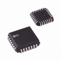
AD1671JP Analog Devices Inc, AD1671JP Datasheet - Page 9

AD1671JP
Manufacturer Part Number
AD1671JP
Description
ADC Single Pipelined 1.25MSPS 12-Bit Parallel 28-Pin PLCC
Manufacturer
Analog Devices Inc
Datasheet
1.AD1671JP.pdf
(16 pages)
Specifications of AD1671JP
Package
28PLCC
Resolution
12 Bit
Sampling Rate
1250 KSPS
Architecture
Pipelined
Number Of Analog Inputs
1
Digital Interface Type
Parallel
Input Type
Voltage
Polarity Of Input Voltage
Unipolar|Bipolar
Rohs Status
RoHS non-compliant
Number Of Bits
12
Sampling Rate (per Second)
1.25M
Data Interface
Parallel
Number Of Converters
2
Power Dissipation (max)
750mW
Voltage Supply Source
Analog and Digital, Dual ±
Operating Temperature
0°C ~ 70°C
Mounting Type
Surface Mount
Package / Case
28-LCC (J-Lead)
Lead Free Status / RoHS Status
Available stocks
Company
Part Number
Manufacturer
Quantity
Price
Part Number:
AD1671JP
Manufacturer:
ADI/亚德诺
Quantity:
20 000
Company:
Part Number:
AD1671JPZ
Manufacturer:
AD
Quantity:
1 000
REV. B
Table I is a list of grounding and decoupling rules that should
be reviewed before laying out a printed circuit board.
Power Supply
Decoupling
Capacitor Values
Capacitor Locations
Reference (REF OUT)
Capacitor Value
Grounding
Analog Ground
Reference Ground
(REF COM)
Digital Ground
Analog and Digital Ground Connected Together Once at the
UNIPOLAR (0 V TO +5 V) CALIBRATION
The AD1671 is factory trimmed to minimize offset, gain and
linearity errors. In some applications the offset and gain errors
of the AD1671 need to be externally adjusted to zero. This is
accomplished by trimming the voltage at AIN2 (Pin 22). The
circuit in Figure 9 is recommended for calibrating offset and
gain errors of the AD1671 when configured in the 0 V to +5 V
input range. If the offset trim resistor R1 is used, it should be
trimmed as follows, although a different offset can be set for a
particular system requirement. This circuit will give approxi-
mately 5 mV of offset trim range. Nominally the AD1671 is
intended to have a 1/2 LSB offset so that the exact analog input
for a given code will be in the middle of that code (halfway be-
tween the transitions to the codes above it and below it). Thus,
the first transition (from 0000 0000 0000 to 0000 0000 0001)
will occur for an input level of +1/2 LSB (0.61 mV for 5 V
range).
Table I. Grounding and Decoupling Guidelines
Comment
0.1 F (Ceramic) and 1 F
(Tantalum) Surface Mount Chip
Capacitors Recommended to
Reduce Lead Inductance
Directly at Positive and Negative
Supply Pins to Common Ground
Plane
1 F (Tantalum) to ACOM
Ground Plane or Wide Ground
Return Connected to the Analog
Power Supply
Critical Common Connections
Should be Star Connected to REF
COM (as Shown in Figure 8)
Ground Plane or Wide Ground
Return Connected to the Digital
Power Supply
AD1671
–9–
The gain trim is done by applying a signal 1 1/2 LSBs below the
nominal full scale (4.998 V for a 5 V range). Trim R2 to give
the last transition (1111 1111 1110 to 1111 1111 1111). This
circuit will give approximately 0.5% FS of adjustment range.
BIPOLAR ( 5 V) CALIBRATION
The connections for the bipolar 5 V input range is shown in
Figure 10.
Bipolar calibration is similar to unipolar calibration. First, a sig-
nal 1/2 LSB above negative full scale (–4.9988 V) is applied and
R1 is trimmed to give the first transition (0000 0000 0000 to
0000 0000 0001). Then a signal 1 1/2 LSB below positive full
scale (+4.9963 V) is applied and R2 is trimmed to give the last
transition (1111 1111 1110 to 1111 1111 1111).
Figure 9. Unipolar (0 V to +5 V) Calibration
OFFSET
OFFSET
–5V TO +5V
0 TO +5V
Figure 10. Bipolar ( 5 V) Calibration
ADJ
ADJ
V
V
IN
IN
10k
10k
R1
R1
+5V
–5V
+5V
–5V
GAIN
GAIN
ADJ
ADJ
50k
50k
25
25
1µF
1µF
R2
50
R2
50
AIN1
AIN2
AIN2
AIN1
SHA OUT
BPO/UPO
REF IN
REF OUT
SHA OUT
BPO/UPO
REF IN
REF OUT
5k
5k
5k
5k
AD1671
AD1671
AD1671
SHA
SHA


