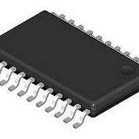
AX5151-TSSOP24-TU AXSEM, AX5151-TSSOP24-TU Datasheet - Page 31

AX5151-TSSOP24-TU
Manufacturer Part Number
AX5151-TSSOP24-TU
Description
RF Transmitter TSSOP-Class-IC
Manufacturer
AXSEM
Type
Single Chip Transceiverr
Datasheet
1.AX5151-TSSOP24-TU.pdf
(43 pages)
Specifications of AX5151-TSSOP24-TU
Package / Case
TSSOP-24
Operating Frequency
400 MHz to 940 MHz
Maximum Operating Temperature
+ 70 C
Mounting Style
SMD/SMT
Operating Supply Voltage
2.3 V to 3.6 V
Supply Current
100 mA
Lead Free Status / RoHS Status
Lead free / RoHS Compliant
5.15. Serial Peripheral Interface (SPI)
The AX5151 can be programmed via a four wire serial interface according SPI using the pins
CLK, MOSI, MISO and SEL. Registers for setting up the AX5151 are programmed via the serial
peripheral interface in all device modes.
When the interface signal SEL is pulled low, a 16 bit configuration data stream is expected on
the input signal pin MOSI, which is interpreted as D0...D7, A0...A6, R_N/W.
Data read from the interface appears on MISO.
Figure 3 shows a write/read access to the interface. The data stream is built of an address
byte including read/write information and a data byte. Depending on the R_N/W bit and
address bits A[6..0], data D[7..0] can be written via MOSI or read at the pin MISO.
R_N/W = 0 means read mode, R_N/W = 1 means write mode.
The read sequence starts with 7 bits of status information S[6..0] followed by 8 data bits.
The status bits contain the following information:
S6
PLL LOCK
SPI Timing
Version 1.0
MOSI
MISO
SCK
SS
Tssd
Tss
R/W
S5
FIFO OVER
A6
S6
Tck TchTcl
A5
S5
A4
S4
S4
FIFO UNDER
Ts
Figure 3 Serial peripheral interface timing
A3
S3
Th
Tco
A2
S2
S3
FIFO FULL
A1
S1
A0
S0
D7
D7
S2
FIFO EMPTY
D6
D6
D5
D5
D4
D4
S1
FIFOSTAT(1)
D3
D3
D2
D2
Circuit Description
Datasheet AX5151
D1
D1
S0
FIFOSTAT(0)
D0
D0
Tsh
Tssz
31


