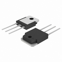
NJW1302G ON Semiconductor, NJW1302G Datasheet

TRANS PNP BIPOLAR 15A 250V TO-3P

NJW1302G

Manufacturer Part Number
NJW1302G
Description
TRANS PNP BIPOLAR 15A 250V TO-3P
Manufacturer
ON Semiconductor
Datasheet

Specifications of NJW1302G

Transistor Type
PNP
Current - Collector (ic) (max)
15A
Voltage - Collector Emitter Breakdown (max)
250V
Vce Saturation (max) @ Ib, Ic
600mV @ 800mA, 8A
Dc Current Gain (hfe) (min) @ Ic, Vce
75 @ 3A, 5V
Power - Max
200W
Frequency - Transition
30MHz
Mounting Type
Through Hole
Package / Case
TO-3P-3, TO-247-3
Transistor Polarity
PNP
Mounting Style
Through Hole
Collector- Emitter Voltage Vceo Max
250 V
Emitter- Base Voltage Vebo
5 V
Maximum Dc Collector Current
15 A
Power Dissipation
200000 mW
Maximum Operating Temperature
+ 150 C
Dc Collector/base Gain Hfe Min
75
Maximum Operating Frequency
30 MHz
Minimum Operating Temperature
- 65 C
Lead Free Status / RoHS Status
Lead free / RoHS Compliant
Current - Collector Cutoff (max)
-
Lead Free Status / Rohs Status
Lead free / RoHS Compliant

Available stocks

Company
Part Number
Manufacturer
Quantity
Price
Part Number:
NJW1302G
Manufacturer:
ON
Quantity:
360
Part Number:
NJW1302G
Manufacturer:
ON
Quantity:
282
Part Number:
NJW1302G
Manufacturer:
ON/安森美
Quantity:
20 000
Company:
Part Number:
NJW1302G
Quantity:
112
NJW3281G (NPN)
NJW1302G (PNP)
Complementary NPN-PNP
Silicon Power Bipolar
Transistors
power audio, disk head positioners and other linear applications.
Features
Benefits
Applications
Stresses exceeding Maximum Ratings may damage the device. Maximum
Ratings are stress ratings only. Functional operation above the Recommended
Operating Conditions is not implied. Extended exposure to stresses above the
Recommended Operating Conditions may affect device reliability.
1. Pulse Test: Pulse Width = 5 ms, Duty Cycle < 10%.
© Semiconductor Components Industries, LLC, 2008
January, 2008 - Rev. 0
MAXIMUM RATINGS
THERMAL CHARACTERISTICS
Collector-Emitter Voltage
Collector-Base Voltage
Emitter-Base Voltage
Collector-Emitter Voltage - 1.5 V
Collector Current
Collector Current
Base Current - Continuous
Total Power Dissipation @ T
Derate Above 25°C
Operating and Storage Junction
Temperature Range
Thermal Resistance, Junction-to-Case
Thermal Resistance, Junction-to-Ambient
The NJW3281G and NJW1302G are power transistors for high
Exceptional Safe Operating Area
NPN/PNP Gain Matching within 10% from 50 mA to 5 A
Excellent Gain Linearity
High BVCEO
High Frequency
These are Pb-Free Devices
Reliable Performance at Higher Powers
Symmetrical Characteristics in Complementary Configurations
Accurate Reproduction of Input Signal
Greater Dynamic Range
High Amplifier Bandwith
High-End Consumer Audio Products
Professional Audio Amplifiers
Home Amplifiers
Home Receivers
Theater and Stadium Sound Systems
Public Address Systems (PAs)
Characteristic
Rating
- Continuous
- Peak (Note 1)
(T
J
= 25°C unless otherwise noted)
C
Preferred Devices
= 25°C
Symbol
Symbol
T
V
V
V
V
R
R
J
P
, T
CEO
CBO
EBO
CEX
I
I
qJC
qJA
C
B
D
stg
- 65 to +150
Value
0.625
1.43
Max
250
250
250
200
5.0
1.6
15
30
40
1
W/°C
°C/W
°C/W
Unit
Unit
Vdc
Vdc
Vdc
Vdc
Adc
Adc
°C
W
Preferred devices are recommended choices for future use
and best overall value.
SILICON POWER TRANSISTORS
NJW3281G
NJW1302G
Device
250 VOLTS 200 WATTS
ORDERING INFORMATION
COMPLEMENTARY
xxxx
G
A
Y
WW
http://onsemi.com
15 AMPERES
(Pb-Free)
(Pb-Free)
STYLES 1,2,3
CASE 340AB
Package
= 0281 or 0302
= Pb-Free Package
= Assembly Location
= Year
= Work Week
TO-3P
TO-3P
TO-3P
Publication Order Number:
30 Units/Rail
30 Units/Rail
MARKING
DIAGRAM
NJWxxxG
Shipping
AYWW
NJW3281/D

Related parts for NJW1302G

NJW1302G Summary of contents

Page 1

... NJW3281G (NPN) NJW1302G (PNP) Preferred Devices Complementary NPN-PNP Silicon Power Bipolar Transistors The NJW3281G and NJW1302G are power transistors for high power audio, disk head positioners and other linear applications. Features • Exceptional Safe Operating Area • NPN/PNP Gain Matching within 10% from • ...

Page 2

... NJW3281G (NPN) NJW1302G (PNP) ELECTRICAL CHARACTERISTICS (T Characteristic OFF CHARACTERISTICS Collector-Emitter Sustaining Voltage (I = 100 mAdc Collector Cutoff Current (V = 250 Vdc Emitter Cutoff Current ( Vdc SECOND BREAKDOWN Second Breakdown Collector with Base Forward Biased ( Vdc (non-repetitive CHARACTERISTICS DC Current Gain (I = 100 mAdc Vdc Adc, V ...

Page 3

... NJW3281G (NPN) NJW1302G (PNP) PNP NJW1302G 25° MHz test 0 COLLECTOR CURRENT (A) C Figure 1. Typical Current Gain Bandwidth Product 1000 125°C 25°C 100 -30°C 10 0.01 0 COLLECTOR CURRENT (A) C Figure 3. DC Current Gain 1000 125°C 25°C 100 -30°C 10 0.01 0 COLLECTOR CURRENT (A) C Figure 5 ...

Page 4

... NJW3281G (NPN) NJW1302G (PNP) PNP NJW1302G 0 0.01 0.001 0. BASE CURRENT (A) B Figure 7. Saturation Region 25°C 0.1 -30°C 125°C 0.01 0.01 0 COLLECTER CURRENT (A) C Figure Collector-Emitter Saturation CE(sat) Voltage 1 1.4 1.2 1.0 0.8 -30°C 0.6 25°C 0.4 125°C ...

Page 5

... NJW3281G (NPN) NJW1302G (PNP) PNP NJW1302G 1200 1000 800 600 400 200 COLLECTER-BASE VOLTAGE (V) CB Figure 13. Output Capacitance 12000 10000 8000 6000 4000 2000 EMITTER-BASE VOLTAGE (V) EB Figure 15. Input Capacitance TYPICAL CHARACTERISTICS 1200 T = 25° MHz Test 1000 800 600 400 ...

Page 6

... Safe operating area curves indicate I limits of the transistor that must be observed for reliable operation; i.e., the transistor must not be subjected to greater dissipation than the curves indicate. NJW3281G (NPN) NJW1302G (PNP) 100 10 mSec 10 100 mSec 1 ...

Page 7

... PUBLICATION ORDERING INFORMATION LITERATURE FULFILLMENT:  Literature Distribution Center for ON Semiconductor  P.O. Box 5163, Denver, Colorado 80217 USA  Phone: 303-675-2175 or 800-344-3860 Toll Free USA/Canada  Fax: 303-675-2176 or 800-344-3867 Toll Free USA/Canada  Email: orderlit@onsemi.com NJW3281G (NPN) NJW1302G (PNP) PACKAGE DIMENSIONS TO-3P-3LD CASE 340AB-01 ISSUE A SEATING A ...

Related keywords