NJW1302G ON Semiconductor, NJW1302G Datasheet - Page 2
NJW1302G
Manufacturer Part Number
NJW1302G
Description
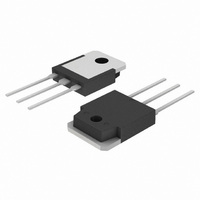
TRANS PNP BIPOLAR 15A 250V TO-3P
Manufacturer
ON Semiconductor
Datasheet
1.NJW1302G.pdf
(7 pages)
Specifications of NJW1302G
Transistor Type
PNP
Current - Collector (ic) (max)
15A
Voltage - Collector Emitter Breakdown (max)
250V
Vce Saturation (max) @ Ib, Ic
600mV @ 800mA, 8A
Dc Current Gain (hfe) (min) @ Ic, Vce
75 @ 3A, 5V
Power - Max
200W
Frequency - Transition
30MHz
Mounting Type
Through Hole
Package / Case
TO-3P-3, TO-247-3
Transistor Polarity
PNP
Mounting Style
Through Hole
Collector- Emitter Voltage Vceo Max
250 V
Emitter- Base Voltage Vebo
5 V
Maximum Dc Collector Current
15 A
Power Dissipation
200000 mW
Maximum Operating Temperature
+ 150 C
Dc Collector/base Gain Hfe Min
75
Maximum Operating Frequency
30 MHz
Minimum Operating Temperature
- 65 C
Lead Free Status / RoHS Status
Lead free / RoHS Compliant
Current - Collector Cutoff (max)
-
Lead Free Status / Rohs Status
Lead free / RoHS Compliant
Available stocks
Company
Part Number
Manufacturer
Quantity
Price

Part Number:
NJW1302G
Manufacturer:
ON/安森美
Quantity:
20 000


ELECTRICAL CHARACTERISTICS
OFF CHARACTERISTICS
SECOND BREAKDOWN
ON CHARACTERISTICS
DYNAMIC CHARACTERISTICS
Collector-Emitter Sustaining Voltage
Collector Cutoff Current
Emitter Cutoff Current
Second Breakdown Collector with Base Forward Biased
DC Current Gain
Collector-Emitter Saturation Voltage
Base-Emitter On Voltage
Current-Gain - Bandwidth Product
Output Capacitance
(I
(V
(V
(V
(I
(I
(I
(I
(I
(I
(I
(I
(V
C
C
C
C
C
C
C
C
C
CB
EB
CE
CB
= 100 mAdc, I
= 100 mAdc, V
= 1 Adc, V
= 3 Adc, V
= 5 Adc, V
= 8 Adc, V
= 8 Adc, I
= 8 Adc, V
= 1 Adc, V
= 5 Vdc, I
= 250 Vdc, I
= 50 Vdc, t = 1 s (non-repetitive)
= 10 Vdc, I
B
CE
CE
CE
CE
CE
CE
= 0.8 Adc)
C
E
= 0)
= 5 Vdc)
= 5 Vdc)
= 5 Vdc)
= 5 Vdc)
= 5 Vdc)
= 5 Vdc, f
B
E
CE
= 0, f
= 0)
= 0)
Characteristic
= 5 Vdc)
test
test
= 1 MHz)
= 1 MHz)
NJW3281G (NPN) NJW1302G (PNP)
(T
C
= 25°C unless otherwise noted)
http://onsemi.com
2
V
Symbol
V
V
CEO(sus)
CE(sat)
I
I
BE(on)
C
CBO
I
h
EBO
S/b
f
FE
T
ob
Min
250
75
75
75
60
45
-
-
4
-
-
-
-
Typ
0.4
30
-
-
-
-
-
-
-
-
-
-
-
Max
150
150
150
600
0.6
1.5
50
-
5
-
-
-
-
mAdc
mAdc
MHz
Unit
Vdc
Adc
Vdc
Vdc
pF
-
Related parts for NJW1302G
Image
Part Number
Description
Manufacturer
Datasheet
Request
R

Part Number:
Description:
ON Semiconductor [VOLTAGE REGULATOR]
Manufacturer:
ON Semiconductor
Datasheet:
Part Number:
Description:
357-036-542-201 CARDEDGE 36POS DL .156 BLK LOPRO
Manufacturer:
ON Semiconductor
Datasheet:
Part Number:
Description:
357-036-542-201 CARDEDGE 36POS DL .156 BLK LOPRO
Manufacturer:
ON Semiconductor
Datasheet:
Part Number:
Description:
357-036-542-201 CARDEDGE 36POS DL .156 BLK LOPRO
Manufacturer:
ON Semiconductor
Datasheet:
Part Number:
Description:
357-036-542-201 CARDEDGE 36POS DL .156 BLK LOPRO
Manufacturer:
ON Semiconductor
Datasheet:
Part Number:
Description:
357-036-542-201 CARDEDGE 36POS DL .156 BLK LOPRO
Manufacturer:
ON Semiconductor
Datasheet:
Part Number:
Description:
357-036-542-201 CARDEDGE 36POS DL .156 BLK LOPRO
Manufacturer:
ON Semiconductor
Datasheet:
Part Number:
Description:
357-036-542-201 CARDEDGE 36POS DL .156 BLK LOPRO
Manufacturer:
ON Semiconductor
Datasheet:
Part Number:
Description:
357-036-542-201 CARDEDGE 36POS DL .156 BLK LOPRO
Manufacturer:
ON Semiconductor
Datasheet:
Part Number:
Description:
357-036-542-201 CARDEDGE 36POS DL .156 BLK LOPRO
Manufacturer:
ON Semiconductor
Datasheet:
Part Number:
Description:
357-036-542-201 CARDEDGE 36POS DL .156 BLK LOPRO
Manufacturer:
ON Semiconductor
Datasheet:
Part Number:
Description:
Manufacturer:
ON Semiconductor
Datasheet:
Part Number:
Description:
Manufacturer:
ON Semiconductor
Datasheet:
Part Number:
Description:
Manufacturer:
ON Semiconductor
Datasheet: