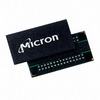
MT46V32M16BN-5B:F Micron Technology Inc, MT46V32M16BN-5B:F Datasheet - Page 57

MT46V32M16BN-5B:F
Manufacturer Part Number
MT46V32M16BN-5B:F
Description
DRAM Chip DDR SDRAM 512M-Bit 32Mx16 2.6V 60-Pin FBGA Tray
Manufacturer
Micron Technology Inc
Type
DDR SDRAMr
Datasheet
1.MT46V32M16P-5BF_TR.pdf
(91 pages)
Specifications of MT46V32M16BN-5B:F
Density
512 Mb
Maximum Clock Rate
400 MHz
Package
60FBGA
Address Bus Width
15 Bit
Operating Supply Voltage
2.6 V
Maximum Random Access Time
0.7 ns
Operating Temperature
0 to 70 °C
Format - Memory
RAM
Memory Type
DDR SDRAM
Memory Size
512M (32Mx16)
Speed
5ns
Interface
Parallel
Voltage - Supply
2.5 V ~ 2.7 V
Package / Case
60-FBGA
Organization
32Mx16
Address Bus
15b
Access Time (max)
700ps
Operating Supply Voltage (typ)
2.6V
Package Type
FBGA
Operating Temp Range
0C to 70C
Operating Supply Voltage (max)
2.7V
Operating Supply Voltage (min)
2.5V
Supply Current
215mA
Pin Count
60
Mounting
Surface Mount
Operating Temperature Classification
Commercial
Lead Free Status / RoHS Status
Lead free / RoHS Compliant
Available stocks
Company
Part Number
Manufacturer
Quantity
Price
Company:
Part Number:
MT46V32M16BN-5B:F
Manufacturer:
MICRON
Quantity:
21
Company:
Part Number:
MT46V32M16BN-5B:F
Manufacturer:
MICRON
Quantity:
513
Company:
Part Number:
MT46V32M16BN-5B:F
Manufacturer:
Micron Technology Inc
Quantity:
10 000
Company:
Part Number:
MT46V32M16BN-5B:F TR
Manufacturer:
Micron Technology Inc
Quantity:
10 000
CAS Latency (CL)
Figure 24:
PDF: 09005aef80a1d9d4/Source: 09005aef82a95a3a
DDR_x4x8x16_Core2.fm - 512Mb DDR: Rev. N; Core DDR Rev. B 2/09 EN
CAS Latency
Note:
The CL is the delay, in clock cycles, between the registration of a READ command and
the availability of the first bit of output data. The latency can be set to 2, 2.5, or 3 (-5B
only) clocks, as shown in Figure 24. Reserved states should not be used, as unknown
operation or incompatibility with future versions may result.
If a READ command is registered at clock edge n, and the latency is m clocks, the data
will be available nominally coincident with clock edge n + m. Table 35 on page 58 indi-
cates the operating frequencies at which each CL setting can be used.
Command
Command
Command
BL = 4 in the cases shown; shown with nominal
DQS
DQS
DQS
CK#
CK#
CK#
DQ
DQ
DQ
CK
CK
CK
READ
READ
READ
T0
T0
T0
CL = 2
CL = 3
CL = 2.5
NOP
NOP
NOP
T1
T1
T1
57
Transitioning Data
Micron Technology, Inc., reserves the right to change products or specifications without notice.
NOP
NOP
NOP
T2
T2
T2
512Mb: x4, x8, x16 DDR SDRAM
T2n
T2n
t
AC,
t
DQSCK, and
NOP
NOP
NOP
T3
T3
T3
Don’t Care
T3n
T3n
T3n
©2000 Micron Technology, Inc. All rights reserved.
t
DQSQ.
Operations


