PCKEL14D-T NXP Semiconductors, PCKEL14D-T Datasheet
PCKEL14D-T
Specifications of PCKEL14D-T


Related parts for PCKEL14D-T


PCKEL14D-T Summary of contents
Page 1
PCKEL14 2.5 V/3.3 V PECL/ECL 1:5 clock distribution chip Rev. 01 — 14 October 2002 1. Description The PCKEL14 is a low skew 1:5 clock distribution chip designed explicitly for low skew clock distribution applications. The device can be driven ...
Page 2
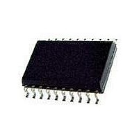
Philips Semiconductors 3. Pinning information 3.1 Pinning Fig 1. SO20 pin configuration. 3.2 Pin description Table 1: Symbol Q0-Q4 Q0- SEL V BB CLK CLK SCLK 3.2.1 Power supply connection CAUTION 9397 750 09564 ...
Page 3
... Philips Semiconductors 4. Ordering information Table 2: Ordering information Type number Package Name Description PCKEL14D SO20 plastic small outline package; 20 leads; body width 7.5 mm PCKEL14PW TSSOP20 plastic thin shrink small outline package; 20 leads; body width 4 Logic diagram Fig 3. Logic diagram. CAUTION 6. Function table Table Don’ ...
Page 4
Philips Semiconductors 7. Limiting values Table 4: Limiting values In accordance with the Absolute Maximum Rating System (IEC 60134). Symbol Parameter V power supply CC V power supply EE V input voltage I I output current sink/source ...
Page 5
Philips Semiconductors 8. Static characteristics Table 5: PECL DC characteristics [ 2 Symbol Parameter I power supply current EE V HIGH-level output OH voltage V LOW-level output OL voltage V HIGH-level ...
Page 6
Philips Semiconductors Table 6: Positive DC characteristics [ 3 Symbol Parameter Conditions I power supply current EE V HIGH-level output OH voltage V LOW-level output OL voltage V HIGH-level input single-ended ...
Page 7
Philips Semiconductors Table 7: Negative DC characteristics 2.375 Symbol Parameter Conditions I power supply EE current V HIGH-level OH output voltage V LOW-level OL output voltage V HIGH-level ...
Page 8
Philips Semiconductors 9. Dynamic characteristics Table 8: AC characteristics (V = 2.375 Symbol Parameter Conditions f maximum toggle see max frequency t LOW-to-HIGH CLK to Q (diff); PLH ...
Page 9
Philips Semiconductors 900 V O (mV p-p ) 800 700 600 500 400 300 200 100 0 Fig 150 mV and 1000 mV input. max 10. Application information Fig 5. Typical termination for output driver and device ...
Page 10
Philips Semiconductors 11. Package outline SO20: plastic small outline package; 20 leads; body width 7 pin 1 index 1 e DIMENSIONS (inch dimensions are derived from the original mm dimensions) A UNIT ...
Page 11
Philips Semiconductors TSSOP20: plastic thin shrink small outline package; 20 leads; body width 4 pin 1 index 1 e DIMENSIONS (mm are the original dimensions) A UNIT max. 0.15 0.95 ...
Page 12
Philips Semiconductors 12. Soldering 12.1 Introduction to soldering surface mount packages This text gives a very brief insight to a complex technology. A more in-depth account of soldering ICs can be found in our Data Handbook IC26; Integrated Circuit Packages ...
Page 13
Philips Semiconductors During placement and before soldering, the package must be fixed with a droplet of adhesive. The adhesive can be applied by screen printing, pin transfer or syringe dispensing. The package can be soldered after the adhesive is cured. ...
Page 14
Philips Semiconductors 14. Data sheet status [1] Level Data sheet status Product status I Objective data Development II Preliminary data Qualification III Product data Production [1] Please consult the most recently issued data sheet before initiating or completing a design. ...
Page 15
Philips Semiconductors Contents 1 Description . . . . . . . . . . . . . . . . . . . . . . . . . . . . . 1 2 Features . . . ...