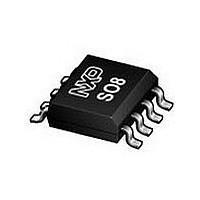
ICM7555CD NXP Semiconductors, ICM7555CD Datasheet - Page 20

ICM7555CD
Manufacturer Part Number
ICM7555CD
Description
Manufacturer
NXP Semiconductors
Type
Standardr
Datasheet
1.ICM7555CD.pdf
(22 pages)
Specifications of ICM7555CD
# Internal Timers
1
Power Dissipation
780mW
Operating Supply Voltage (min)
3V
Operating Supply Voltage (typ)
3.3/5/9/12/15V
Operating Supply Voltage (max)
16V
Package Type
SO
High Level Output Current
-1mA
Low Level Output Current
3.2mA
Pin Count
8
Operating Temp Range
0C to 70C
Operating Temperature Classification
Commercial
Mounting
Surface Mount
Lead Free Status / RoHS Status
Compliant
Available stocks
Company
Part Number
Manufacturer
Quantity
Price
Company:
Part Number:
ICM7555CD
Manufacturer:
NXP
Quantity:
1 945
Part Number:
ICM7555CD
Manufacturer:
NXP/恩智浦
Quantity:
20 000
Part Number:
ICM7555CD/01
Manufacturer:
NXP/恩智浦
Quantity:
20 000
Company:
Part Number:
ICM7555CD/01,118
Manufacturer:
Intel
Quantity:
52
Company:
Part Number:
ICM7555CD/01118
Manufacturer:
NXP Semiconductors
Quantity:
269 796
NXP Semiconductors
16. Revision history
Table 10.
ICM7555_2
Product data sheet
Document ID
ICM7555_2
Modifications:
ICM7555_1
Revision history
Release date
20090803
19940831
•
•
•
•
•
•
•
•
•
•
The format of this data sheet has been redesigned to comply with the new identity guidelines of NXP
Semiconductors.
Legal texts have been adapted to the new company name where appropriate.
Provided separate pinning diagrams for SO8 and DIP8 packages
respectively).
Added
Table 4 “Limiting
– Symbols V
– Symbol/parameter “P
– Symbol/parameter “T
– Symbol changed from “T
Table 5
– Symbols f/f, f/ V, f/ T, have been added for Astable mode timing.
– Symbols V
– Symbols I
– Symbol/parameter “V
– Symbol/parameter “t
– Symbol/parameter “t
– Symbol “F
Section 11.4 “Astable
Added
Added soldering information.
Added
Conditions column).
maximum values given).
Conditions column).
column).
name is now noted under Conditions column).
Table 2 “Pin
Section 12 “Package
Section 15
“Characteristics”:
TRIG
MAX
TRIG
TRIG
Data sheet status
Product data sheet
Product specification
values”:
, I
” changed to “f
, V
, V
“Abbreviations”.
TH
description”.
CV
CV
, I
operation”: changed symbol for duty cycle from “D” to “ ”.
, V
, V
RST
R
F
STG
DMAX
DIS
, fall time of output” changed to “t
, rise time of output” changed to “t
TH
TH
are replaced with I
, discharge output voltage” changed to “V
Rev. 02 — 3 August 2009
, storage temperature range” replaced with “T
SOLD
, V
, V
outline”.
, maximum power dissipation” replaced with “P, power dissipation” (only
RST
RST
osc
” to “T
, oscillator frequency”.
are replaced with V
are replaced with V
sp
, solder point temperature”
I
(specific pin names are now noted under Conditions
Change notice
-
ECN 853-1192 13721
dated 1994 Aug 31
I
I
(specific pin names are now noted under
(specific pin names are now noted under
f(o)
r(o)
, output fall time”.
, output rise time”.
(Figure 2
General purpose CMOS timer
o
, output voltage” (specific pin
stg
and
, storage temperature”.
Supersedes
ICM7555_1
-
Figure
© NXP B.V. 2009. All rights reserved.
ICM7555
3,
20 of 22


