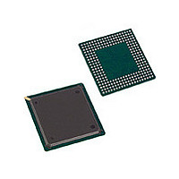
CYP15G0402DXB-BGI Cypress Semiconductor Corp, CYP15G0402DXB-BGI Datasheet - Page 29

CYP15G0402DXB-BGI
Manufacturer Part Number
CYP15G0402DXB-BGI
Description
Manufacturer
Cypress Semiconductor Corp
Datasheet
1.CYP15G0402DXB-BGI.pdf
(29 pages)
Specifications of CYP15G0402DXB-BGI
Lead Free Status / RoHS Status
Not Compliant
Document #: 38-02057 Rev. *G
Document History Page
Document Title:CYP(V)15G0402DXB Quad HOTLink II™ SERDES
Document Number: 38-02057
REV.
*C
*D
*G
*A
*B
*E
*F
**
ECN NO. Issue Date
116285
118985
122545
122211
124992
128367
131899
338721
See ECN
07/16/02
09/30/02
12/09/02
12/28/02
04/15/03
07/24/03
01/21/04
Change
Orig. of
SDR
LNM
CGX
POT
PDS
PDS
SUA
RBI
New Data Sheet
Changed TXCLKO description
Changed TXPERx description
introduced SMPTE pathological test clause
Removed the LOW setting for FRAMCHAR and related references
Changed V
Changed the I
Changed the t
Changed t
Changed t
Changed the JTAG ID from 0C801069 to 1C801069
Changed Minimum tRISE/tFALL for CML
Changed tTXCLKOD+, tTXCLKOD- for LVTTL
Changed tRXLOCK
Changed tDJ, tRJ
Changed tJTOL
Changed tTXLOCK
Changed tRXCLKH, tRXCLKL
Changed Power Specs
Changed verbiage...Paragraph: Clock/Data Recovery
Changed verbiage...Paragraph: Range Control
Updated differences to pin configuration and pin table
Added Power-up Requirements
Minor change Document Control corrected Document History Page
Changed CYP15G0402DXB to CYP(V)15G0402DXB type corresponding to
Video-compliant parts
Reduced the lower limit of the serial signaling rate from 200 Mbaud to
195 Mbaud and changed the associated specifications accordingly
Added t
Removed irrelevant timing parameters
When TXCKSEL = MID or HIGH, TXRATE = HIGH is an invalid mode. Made
appropriate changes to reflect this invalid condition
Changed LFIx to Asynchronous output
Expanded the CDR Range Controller’s permissible frequency offset between
incoming serial signaling rate and Reference clock from ±200-PPM to
±1500-PPM (changed parameter t
Revised Typical Power numbers to match final characterization data
Added Pb-Free Package option availability
Changed MBd to MBaud in SPDSEL pin description
RXDV+
TXDS
REFADV–
ODIF
OST
TXCLKR
timing parameter
and t
and V
boundary values
and t
TXDH
OLC
and t
REFCDV–
and t
for CML output
Description of Change
TXCLKF
TREFDS
and t
min values
REFRX
and t
REFCDV+
)
TREFDH
CYP15G0402DXB
CYV15G0402DXB
Page 29 of 29
[+] Feedback


