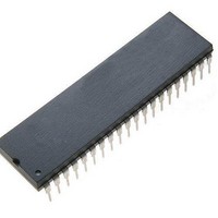
PIC16F1517-E/P Microchip Technology, PIC16F1517-E/P Datasheet - Page 144

PIC16F1517-E/P
Manufacturer Part Number
PIC16F1517-E/P
Description
40-pin, 14KB Flash, 512B RAM, 10-bit ADC, 2xCCP, SPI, MI2C, EUSART, 2.3V-5.5V 40
Manufacturer
Microchip Technology
Series
PIC® XLP™ 16Fr
Datasheet
1.PIC16F1516-EMV.pdf
(344 pages)
Specifications of PIC16F1517-E/P
Processor Series
PIC16F151x
Core
PIC
Data Bus Width
8 bit
Program Memory Type
Flash
Program Memory Size
8 KB
Data Ram Size
512 B
Interface Type
I2C, SPI, USART
Maximum Clock Frequency
20 MHz
Number Of Programmable I/os
36
Number Of Timers
3
Operating Supply Voltage
2.3 V to 5.5 V
Maximum Operating Temperature
+ 125 C
Mounting Style
Through Hole
Package / Case
PDIP-40
Core Processor
PIC
Core Size
8-Bit
Speed
20MHz
Connectivity
I²C, LIN, SPI, UART/USART
Peripherals
Brown-out Detect/Reset, POR, PWM, WDT
Number Of I /o
36
Eeprom Size
-
Ram Size
512 x 8
Voltage - Supply (vcc/vdd)
2.3 V ~ 5.5 V
Data Converters
A/D 28x10b
Oscillator Type
Internal
Operating Temperature
-40°C ~ 125°C
Lead Free Status / Rohs Status
Details
Available stocks
Company
Part Number
Manufacturer
Quantity
Price
Company:
Part Number:
PIC16F1517-E/PT
Manufacturer:
Microchip Technology
Quantity:
10 000
- Current page: 144 of 344
- Download datasheet (3Mb)
PIC16(L)F1516/7/8/9
16.1.5
The ADC module allows for the ability to generate an
interrupt upon completion of an Analog-to-Digital
conversion. The ADC Interrupt Flag is the ADIF bit in
the PIR1 register. The ADC Interrupt Enable is the
ADIE bit in the PIE1 register. The ADIF bit must be
cleared in software.
This interrupt can be generated while the device is
operating or while in Sleep. If the device is in Sleep, the
interrupt will wake-up the device. Upon waking from
Sleep, the next instruction following the SLEEP instruc-
tion is always executed. If the user is attempting to
wake-up from Sleep and resume in-line code execu-
tion, the GIE and PEIE bits of the INTCON register
must be disabled. If the GIE and PEIE bits of the
INTCON register are enabled, execution will switch to
the Interrupt Service Routine.
FIGURE 16-3:
DS41452B-page 144
Note 1: The ADIF bit is set at the completion of
(ADFM = 0)
(ADFM = 1)
2: The ADC operates during Sleep only
INTERRUPTS
every conversion, regardless of whether
or not the ADC interrupt is enabled.
when the F
10-BIT A/D CONVERSION RESULT FORMAT
MSB
bit 7
bit 7
RC
Unimplemented: Read as ‘0’
oscillator is selected.
ADRESH
10-bit A/D Result
Preliminary
MSB
bit 0
bit 0
16.1.6
The 10-bit A/D conversion result can be supplied in two
formats, left justified or right justified. The ADFM bit of
the ADCON1 register controls the output format.
Figure 16-3
bit 7
bit 7
RESULT FORMATTING
shows the two output formats.
10-bit A/D Result
LSB
Unimplemented: Read as ‘0’
2011 Microchip Technology Inc.
ADRESL
bit 0
LSB
bit 0
Related parts for PIC16F1517-E/P
Image
Part Number
Description
Manufacturer
Datasheet
Request
R

Part Number:
Description:
IC, 8BIT MCU, PIC16F, 32MHZ, SOIC-18
Manufacturer:
Microchip Technology
Datasheet:

Part Number:
Description:
IC, 8BIT MCU, PIC16F, 32MHZ, SSOP-20
Manufacturer:
Microchip Technology
Datasheet:

Part Number:
Description:
IC, 8BIT MCU, PIC16F, 32MHZ, DIP-18
Manufacturer:
Microchip Technology
Datasheet:

Part Number:
Description:
IC, 8BIT MCU, PIC16F, 32MHZ, QFN-28
Manufacturer:
Microchip Technology
Datasheet:

Part Number:
Description:
IC, 8BIT MCU, PIC16F, 32MHZ, QFN-28
Manufacturer:
Microchip Technology
Datasheet:

Part Number:
Description:
IC, 8BIT MCU, PIC16F, 32MHZ, QFN-28
Manufacturer:
Microchip Technology
Datasheet:

Part Number:
Description:
IC, 8BIT MCU, PIC16F, 32MHZ, SSOP-20
Manufacturer:
Microchip Technology
Datasheet:

Part Number:
Description:
IC, 8BIT MCU, PIC16F, 20MHZ, DIP-40
Manufacturer:
Microchip Technology
Datasheet:

Part Number:
Description:
IC, 8BIT MCU, PIC16F, 32MHZ, QFN-28
Manufacturer:
Microchip Technology
Datasheet:

Part Number:
Description:
IC, 8BIT MCU, PIC16F, 20MHZ, MQFP-44
Manufacturer:
Microchip Technology
Datasheet:

Part Number:
Description:
IC, 8BIT MCU, PIC16F, 20MHZ, QFN-20
Manufacturer:
Microchip Technology
Datasheet:

Part Number:
Description:
IC, 8BIT MCU, PIC16F, 32MHZ, QFN-28
Manufacturer:
Microchip Technology
Datasheet:

Part Number:
Description:
MCU 14KB FLASH 768B RAM 64-TQFP
Manufacturer:
Microchip Technology
Datasheet:

Part Number:
Description:
7 KB Flash, 384 Bytes RAM, 32 MHz Int. Osc, 16 I/0, Enhanced Mid Range Core, Low
Manufacturer:
Microchip Technology

Part Number:
Description:
14KB Flash, 512B RAM, 256B EEPROM, LCD, 1.8-5.5V 40 UQFN 5x5x0.5mm TUBE
Manufacturer:
Microchip Technology
Datasheet:


