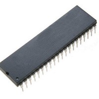
PIC16F1517-E/P Microchip Technology, PIC16F1517-E/P Datasheet - Page 98

PIC16F1517-E/P
Manufacturer Part Number
PIC16F1517-E/P
Description
40-pin, 14KB Flash, 512B RAM, 10-bit ADC, 2xCCP, SPI, MI2C, EUSART, 2.3V-5.5V 40
Manufacturer
Microchip Technology
Series
PIC® XLP™ 16Fr
Datasheet
1.PIC16F1516-EMV.pdf
(344 pages)
Specifications of PIC16F1517-E/P
Processor Series
PIC16F151x
Core
PIC
Data Bus Width
8 bit
Program Memory Type
Flash
Program Memory Size
8 KB
Data Ram Size
512 B
Interface Type
I2C, SPI, USART
Maximum Clock Frequency
20 MHz
Number Of Programmable I/os
36
Number Of Timers
3
Operating Supply Voltage
2.3 V to 5.5 V
Maximum Operating Temperature
+ 125 C
Mounting Style
Through Hole
Package / Case
PDIP-40
Core Processor
PIC
Core Size
8-Bit
Speed
20MHz
Connectivity
I²C, LIN, SPI, UART/USART
Peripherals
Brown-out Detect/Reset, POR, PWM, WDT
Number Of I /o
36
Eeprom Size
-
Ram Size
512 x 8
Voltage - Supply (vcc/vdd)
2.3 V ~ 5.5 V
Data Converters
A/D 28x10b
Oscillator Type
Internal
Operating Temperature
-40°C ~ 125°C
Lead Free Status / Rohs Status
Details
Available stocks
Company
Part Number
Manufacturer
Quantity
Price
Company:
Part Number:
PIC16F1517-E/PT
Manufacturer:
Microchip Technology
Quantity:
10 000
- Current page: 98 of 344
- Download datasheet (3Mb)
PIC16(L)F1516/7/8/9
TABLE 11-1:
11.2.1
To read a program memory location, the user must:
1.
2.
3.
Once the read control bit is set, the program memory
Flash controller will use the second instruction cycle to
read the data. This causes the second instruction
immediately following the “BSF PMCON1,RD” instruction
to be ignored. The data is available in the very next cycle,
in the PMDATH:PMDATL register pair; therefore, it can
be read as two bytes in the following instructions.
PMDATH:PMDATL register pair will hold this value until
another read or until it is written to by the user.
DS41452B-page 98
Note:
PIC16(L)F1516
PIC16(L)F1517
PIC16(L)F1518
PIC16(L)F1519
Write
PMADRH:PMADRL register pair.
Clear the CFGS bit of the PMCON1 register.
Then, set control bit RD of the PMCON1 register.
Device
READING THE FLASH PROGRAM
MEMORY
The two instructions following a program
memory read are required to be NOPs.
This prevents the user from executing a
two-cycle
instruction after the RD bit is set.
the
FLASH MEMORY
ORGANIZATION BY DEVICE
desired
instruction
Row Erase
(words)
32
address
on
Latches
(words)
the
to
Write
32
the
next
Preliminary
FIGURE 11-1:
Program or Configuration Memory
Instruction Fetched ignored
Instruction Fetched ignored
Initiate READ operation
NOP execution forced
NOP execution forced
(PMADRH:PMADRL)
PMDATH:PMDATL
READ Operation
Data read now in
READ Operation
Word Address
FLASH PROGRAM
MEMORY READ
FLOWCHART
2011 Microchip Technology Inc.
(RD = 1)
(CFGS)
Select
Select
Start
End
Related parts for PIC16F1517-E/P
Image
Part Number
Description
Manufacturer
Datasheet
Request
R

Part Number:
Description:
IC, 8BIT MCU, PIC16F, 32MHZ, SOIC-18
Manufacturer:
Microchip Technology
Datasheet:

Part Number:
Description:
IC, 8BIT MCU, PIC16F, 32MHZ, SSOP-20
Manufacturer:
Microchip Technology
Datasheet:

Part Number:
Description:
IC, 8BIT MCU, PIC16F, 32MHZ, DIP-18
Manufacturer:
Microchip Technology
Datasheet:

Part Number:
Description:
IC, 8BIT MCU, PIC16F, 32MHZ, QFN-28
Manufacturer:
Microchip Technology
Datasheet:

Part Number:
Description:
IC, 8BIT MCU, PIC16F, 32MHZ, QFN-28
Manufacturer:
Microchip Technology
Datasheet:

Part Number:
Description:
IC, 8BIT MCU, PIC16F, 32MHZ, QFN-28
Manufacturer:
Microchip Technology
Datasheet:

Part Number:
Description:
IC, 8BIT MCU, PIC16F, 32MHZ, SSOP-20
Manufacturer:
Microchip Technology
Datasheet:

Part Number:
Description:
IC, 8BIT MCU, PIC16F, 20MHZ, DIP-40
Manufacturer:
Microchip Technology
Datasheet:

Part Number:
Description:
IC, 8BIT MCU, PIC16F, 32MHZ, QFN-28
Manufacturer:
Microchip Technology
Datasheet:

Part Number:
Description:
IC, 8BIT MCU, PIC16F, 20MHZ, MQFP-44
Manufacturer:
Microchip Technology
Datasheet:

Part Number:
Description:
IC, 8BIT MCU, PIC16F, 20MHZ, QFN-20
Manufacturer:
Microchip Technology
Datasheet:

Part Number:
Description:
IC, 8BIT MCU, PIC16F, 32MHZ, QFN-28
Manufacturer:
Microchip Technology
Datasheet:

Part Number:
Description:
MCU 14KB FLASH 768B RAM 64-TQFP
Manufacturer:
Microchip Technology
Datasheet:

Part Number:
Description:
7 KB Flash, 384 Bytes RAM, 32 MHz Int. Osc, 16 I/0, Enhanced Mid Range Core, Low
Manufacturer:
Microchip Technology

Part Number:
Description:
14KB Flash, 512B RAM, 256B EEPROM, LCD, 1.8-5.5V 40 UQFN 5x5x0.5mm TUBE
Manufacturer:
Microchip Technology
Datasheet:


