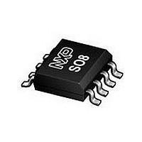
PCF8563TF4 NXP Semiconductors, PCF8563TF4 Datasheet - Page 17

PCF8563TF4
Manufacturer Part Number
PCF8563TF4
Description
Manufacturer
NXP Semiconductors
Datasheet
1.PCF8563TF4.pdf
(45 pages)
Specifications of PCF8563TF4
Bus Type
Serial (2-Wire, I2C)
Operating Supply Voltage (typ)
2.5/3.3/5V
Package Type
SO
Operating Supply Voltage (max)
5.5V
Operating Supply Voltage (min)
1.8V
Operating Temperature Classification
Industrial
Operating Temperature (max)
85C
Operating Temperature (min)
-40C
Pin Count
8
Mounting
Surface Mount
Date Format
DW:DM:M:Y
Time Format
HH:MM:SS
Lead Free Status / RoHS Status
Compliant
Available stocks
Company
Part Number
Manufacturer
Quantity
Price
NXP Semiconductors
PCF8563
Product data sheet
8.8.2 Register Timer
8.9.1 Operation example:
8.9 EXT_CLK test mode
Table 24.
Table 25.
The register Timer is an 8-bit binary countdown timer. It is enabled and disabled via the
Timer_control register bit TE. The source clock for the timer is also selected by the
Timer_control register. Other timer properties such as interrupt generation are controlled
via the register Control_status
For accurate read back of the count down value, it is recommended to read the register
twice and check for consistent results, since it is not possible to freeze the countdown
timer counter during read back.
A test mode is available which allows for on-board testing. In such a mode it is possible to
set up test conditions and control the operation of the RTC.
The test mode is entered by setting bit TEST1 in register Control_status_1. Then
pin CLKOUT becomes an input. The test mode replaces the internal 64 Hz signal with the
signal applied to pin CLKOUT. Every 64 positive edges applied to pin CLKOUT will then
generate an increment of one second.
The signal applied to pin CLKOUT should have a minimum pulse width of 300 ns and a
maximum period of 1000 ns. The internal 64 Hz clock, now sourced from CLKOUT, is
divided down to 1 Hz by a 2
a known state by using bit STOP. When bit STOP is set, the prescaler is reset to 0 (STOP
must be cleared before the prescaler can operate again).
From a STOP condition, the first 1 second increment will take place after 32 positive
edges on CLKOUT. Thereafter, every 64 positive edges will cause a one-second
increment.
Remark: Entry into EXT_CLK test mode is not synchronized to the internal 64 Hz clock.
When entering the test mode, no assumption as to the state of the prescaler can be made.
Bit
7 to 0
Bit
7
128
1. Set EXT_CLK test mode (Control_status_1, bit TEST1 = 1).
2. Set STOP (Control_status_1, bit STOP = 1).
3. Clear STOP (Control_status_1, bit STOP = 0).
4. Set time registers to desired value.
Symbol
TIMER[7:0]
Timer - timer value register (address 0Fh) bit description
Timer register bits value range
6
64
All information provided in this document is subject to legal disclaimers.
Rev. 8 — 18 November 2010
5
32
Value
00h to FFh
6
divide chain called a prescaler. The prescaler can be set into
_
2.
4
16
Description
countdown period in seconds:
where n is the countdown value
CountdownPeriod
3
8
2
4
=
Real-time clock/calendar
-------------------------------------------------------------- -
SourceClockFrequency
1
2
PCF8563
© NXP B.V. 2010. All rights reserved.
n
0
1
17 of 45


