HV256FG-G Supertex, HV256FG-G Datasheet - Page 6
HV256FG-G
Manufacturer Part Number
HV256FG-G
Description
Op Amps 32-Ch MEMS Drvr IC
Manufacturer
Supertex
Datasheet
1.HV256FG-G.pdf
(13 pages)
Specifications of HV256FG-G
Operating Temperature (max)
85C
Operating Temperature Classification
Commercial
Mounting
Surface Mount
Maximum Operating Temperature
+ 85 C
Mounting Style
SMD/SMT
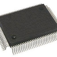
Package / Case
MQFP-100
Minimum Operating Temperature
- 10 C
Lead Free Status / RoHS Status
Compliant


RSINK / RSOURCE
The VDD_BYP, VDD_BYP, and VNN_BYP pins are internal, high
impedance current, mirror gate nodes, brought out to mantain stable
opamp biasing currents in noisy power supply environments. 0.1uF/
25V bypass capacitors, added from the VPP_BYP pin to VPP, from
VDD_BYP pin to VDD, and from VNN_BYP to VNN, will force the
Typical Characteristics
600
500
400
300
200
100
0
25k
BYP _ VNN Cap
BYP _ VPP Cap
BYP_ VDD Cap
0.1uF / 25V
0.1uF / 25V
0.1uF / 25V
(V
PP
= 300V, V
I
DD
SINK vs
BYP _ VPP
BYP _ VNN
BYP_ VDD
R
= 6.5V, V
SINK
VDD
150k
VNN
VPP
R
(KΩ)
NN
SINK
●
= 5.5V, T
1235 Bordeaux Drive, Sunnyvale, CA 94089
max
min
A
= 25
O
C)
Set by RSOURCE
To internal biasing
Set by RSINK
250k
6
high impedance gate nodes to follow the fluctuation of power lines.
The expected voltages at the VDD_BYP, and VNN_BYP pins are
typically 1.5 volts from their respectful power supply. The expected
voltage at VPP_BYP is typically 3.0V below V
600
500
400
300
200
100
0
HVOpamp
●
25k
Tel: 408-222-8888
Current limit
HV
Current limit
OUT
(V
PP
0
= 300V, V
I
SOURCE vs
R
DD
●
HVOpamp
SOURCE
= 6.5V, V
www.supertex.com
150k
R
NN
SOURCE
(KΩ)
= 5.5V, T
HV
max
min
A
= 25
PP
OUT
.
O
C)
31
HV256
250k
Related parts for HV256FG-G
Image
Part Number
Description
Manufacturer
Datasheet
Request
R

Part Number:
Description:
32-channel High Voltage Amplifier Array
Manufacturer:
Supertex, Inc.
Datasheet:
Part Number:
Description:
32-channel Serial To Parallel Converter With High Voltage Push-pull Outputs - Supertex, Inc
Manufacturer:
Supertex, Inc.
Datasheet:
