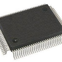
HV257FG-G Supertex, HV257FG-G Datasheet

HV257FG-G
Specifications of HV257FG-G
Available stocks
Related parts for HV257FG-G
HV257FG-G Summary of contents
Page 1
... Typical Application Circuit DAC Micro Processor 32-Channel High Voltage General Description The Supertex HV257 is a 32-channel, high voltage, sample and hold amplifier array integrated circuit. It operates on a single high voltage supply 300V, and two low voltage supplies All 32 sample and hold circuits share a common analog input, V ...
Page 2
... Ordering Information 100-Lead MQFP 20.00x14.00mm body Device 3.15mm height (max) 3.20mm footprint HV257 HV257FG-G -G indicates package is RoHS compliant (‘Green’) Absolute Maximum Ratings Parameter V , High voltage supply Analog low voltage positive supply Digital low voltage positive supply Analog low voltage negative supply ...
Page 3
Electrical Characteristics High Voltage Amplifier Sym Parameter HV HV voltage swing OUT OUT V Input offset INOS HV slew rate rise OUT SR HV slew rate fall OUT BW HV -3dB channel bandwidth OUT A Open loop gain O A ...
Page 4
Decoder Truth Table ↕ ↕ Sample and Hold Timing A0-A4 HVOpamp Temperature Diode Sym Parameter PIV Peak inverse voltage V Forward diode ...
Page 5
Block Diagram BYP-AVDD BYP-VPP VPP AVDD Bias Circuit AVNN DVDD DVNN VSIG Decoder DGND AGND HV OUT Current ...
Page 6
Power Up/Down Issues External Diode Protection The device can be damaged due to improper power up / down sequence. To prevent damage, please follow the acceptable power up / down sequences, and add two external diodes as shown in the ...
Page 7
RSINK / RSOURCE The VDD_BYP, VDD_BYP, and VNN_BYP pins are internal, high impedance current, mirror gate nodes, brought out to mantain stable opamp biasing currents in noisy power supply environments. 0.1uF/25V bypass capacitors, added from VPP_BYP pin to VPP, from ...
Page 8
Typical Characteristics I R SINK 300V 6.5V 600 500 400 300 200 100 0 25k 150k R (KΩ) SINK Acquisition Window (”one RC” response to one volt input step ...
Page 9
Typical Characteristics (cont.) V PSRR vs Frequency 300V 6.5V -50 -40 -30 -20 - 100 1k Frequency (Hz) V PSRR vs Frequency 300V 6.5V, ...
Page 10
Pad Configuration (not drawn to scale) Anode Cathode RSINK RSOURCE BYP-VPP VPP HV OUT31 HV OUT30 HV OUT29 HV OUT28 HV OUT27 HV OUT26 HV OUT25 HV OUT24 HV OUT23 HV OUT22 HV OUT21 HV OUT20 HV OUT19 HV OUT18 ...
Page 11
Pad Coordinates Chip size: 17160μm x 5830μm Center of die is (0,0) Pad Name X (μm) Y (μm) VPP -8338.5 2708 -7895.0 2305.5 OUT HV 1 7448.5 2305.5 OUT HV 2 -7001.5 2305.5 OUT HV 3 -6554.5 2305.5 ...
Page 12
Pin Description Pin # Function Description OUT OUT OUT OUT OUT OUT OUT OUT 9 HV ...
Page 13
Pin Description (cont.) Pin # Function Description 34- connect 39 AGND Analog ground. There are three pads. They need to be externally connected. Analog low voltage negative supply. This should be at the same potential as DVNN. There ...
Page 14
Pin Description (cont.) Pin # Function Description External resistor from RSINK to VNN sets output current sinking limit. Current limit is 97 RSINK approximately 12.5V divided by RSINK resistor value. External resistor from RSOURCE to VNN sets output current sourcing ...
Page 15
... Supertex inc. does not recommend the use of its products in life support applications, and will not knowingly sell them for use in such applications unless it receives an adequate “product liability indemnification insurance agreement.” Supertex inc. does not assume responsibility for use of devices described, and limits its liability to the replacement of the devices determined defective due to workmanship ...


