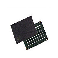
MT45W2MW16PGA-70 IT Micron Technology Inc, MT45W2MW16PGA-70 IT Datasheet - Page 5

MT45W2MW16PGA-70 IT
Manufacturer Part Number
MT45W2MW16PGA-70 IT
Description
Manufacturer
Micron Technology Inc
Datasheet
1.MT45W2MW16PGA-70_IT.pdf
(26 pages)
Specifications of MT45W2MW16PGA-70 IT
Operating Temperature (max)
85C
Operating Temperature (min)
-40C
Mounting
Surface Mount
Operating Temperature Classification
Industrial
Lead Free Status / RoHS Status
Compliant
General Description
Functional Block Diagram
Figure 2:
PDF: 09005aef82832fa7 / Source: 09005aef82832f97
32mb_asyncpage_cr1_0_p24z_2.fm - Rev. B 12/09 EN
Functional Block Diagram 2 Meg x 16
Note:
Micron
for low-power, portable applications. The MT45W2MW16P is a 32Mb DRAM core device
organized as 2 Meg x 16 bits. These devices include the industry-standard, asynchronous
memory interface found on other low-power SRAM or pseudo-SRAM offerings.
A user-accessible configuration register (CR) defines how the CellularRAM device
performs on-chip refresh and whether page mode read accesses are permitted. This
register is automatically loaded with a default setting during power-up and can be
updated at any time during normal operation.
For seamless operation on an asynchronous memory bus, CellularRAM products incor-
porate a transparent self-refresh mechanism. The hidden refresh requires no additional
support from the system memory controller and has no significant impact on device
read/write performance.
Special attention has been focused on current consumption during self refresh. Cellu-
larRAM products include three system-accessible mechanisms to minimize refresh
current. Temperature-compensated refresh (TCR) uses an on-chip sensor to adjust the
refresh rate to match the device temperature. The refresh rate decreases at lower
temperatures to minimize current consumption during standby. Setting sleep enable
(ZZ#) to LOW enables one of two low-power modes: partial-array refresh (PAR) or deep
power-down (DPD). PAR limits refresh to only that part of the DRAM array that contains
essential data. DPD halts refresh operation altogether and is used when no vital infor-
mation is stored in the device. The system-configurable refresh mechanisms are
accessed through the CR.
WE#
OE#
UB#
CE#
LB#
ZZ#
Functional block diagrams illustrate simplified device operation. See ball description table,
bus operations table, and timing diagrams for detailed information.
A[20:0]
®
CellularRAM™ products are high-speed, CMOS PSRAM memories developed
Control
Logic
32Mb: 2 Meg x 16 Async/Page CellularRAM 1.0 Memory
Address Decode
Configuration
Register (CR)
5
Logic
Micron Technology, Inc., reserves the right to change products or specifications without notice.
2,048K x 16
Memory
DRAM
Array
General Description
©2007 Micron Technology, Inc. All rights reserved.
Output
Buffers
Input/
MUX
and
DQ[7:0]
DQ[15:8]


