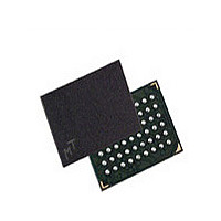
MT45W512KW16PGA-70 WT Micron Technology Inc, MT45W512KW16PGA-70 WT Datasheet
MT45W512KW16PGA-70 WT
Specifications of MT45W512KW16PGA-70 WT


Related parts for MT45W512KW16PGA-70 WT


MT45W512KW16PGA-70 WT Summary of contents
Page 1
... Micron without notice. Products are only warranted by Micron to meet Micron’s production data sheet specifications. 8Mb: 512K x 16 Async/Page PSRAM www.micron.com/products/psram/ Figure Designator MT45W512KW16P GA MT45W512KW16PGA-70WT – Micron Technology, Inc., reserves the right to change products or specifications without notice. 1 Advance ‡ Features Ball Assignment – 48-Ball VFBGA ...
Page 2
General Description Micron low-power, portable applications. The MT45W512KW16P is an 8Mb DRAM core device organized as 512K x 16 bits. These devices include the industry-standard, asynchronous memory interface found on other low-power SRAM or PSRAM offerings. A user-accessible configuration register ...
Page 3
Ball Descriptions Table 1: VFBGA Ball Descriptions VFBGA Ball Assignment Symbol Type H1, D3, E4, F4, A[18:0] Input F3, G4, G3, H5, H4, H3, H2, D4, C4, C3, B4, B3, A5, A4 ZZ# Input B5 CE# Input A2 ...
Page 4
Bus Operations Table 2: Bus Operations Mode Power Standby Standby Read Active Write Active Idle No operation PAR Partial-array refresh DPD Deep power-down Active Load configuration register Notes: 1. When the device is in standby mode, control inputs (WE#, OE#), ...
Page 5
Part Numbering Information Micron PSRAM devices are available in several different configurations and densities (see Figure 3). Figure 3: Part Number Chart 512K W Micron Technology Product Family ® PSRAM/CellularRAM Memory Operating Core Voltage W ...
Page 6
Functional Description In general, the MT45W512KW16P device is a high-density alternative to SRAM and PSRAM products, popular in low-power, portable applications. The MT45W512KW16P contains an 8,388,608-bit DRAM core organized as 524,288 addresses by 16 bits. These devices include the industry-standard, ...
Page 7
Figure 5: READ Operation CE# OE# WE# ADDRESS DATA LB#/UB# Figure 6: WRITE Operation CE# OE# WE# ADDRESS DATA LB#/UB# PDF: 09005aef8220472e/Source: 09005aef8220461e 8mb_asyncpage_ps1_0_p23z.fm - Rev. A 7/06 EN 8Mb: 512K x 16 Async/Page PSRAM ADDRESS VALID DATA VALID t ...
Page 8
Page Mode READ Operation Page mode is a performance-enhancing extension to the legacy asynchronous READ operation. In page-mode-capable products, an initial asynchronous read access is performed. Adjacent addresses can then be quickly read by simply changing the low- order address. ...
Page 9
Low-Power Operation Standby Mode Operation During standby, the device current consumption is reduced to the level necessary to perform the DRAM refresh operation on the full array. Standby operation occurs when CE# and ZZ# are HIGH. The device will enter ...
Page 10
Figure 8: Software Access PAR Functionality NO Deep Power-Down (DPD) Operation DPD operation disables all refresh-related activity. This mode is used when the system does not require the storage provided by the PSRAM device. Any stored data will become corrupted ...
Page 11
Configuration Register (CR) Operation The CR defines how the PSRAM device performs its transparent self refresh. Altering the refresh parameters can dramatically reduce current consumption during standby mode. Page mode control is also embedded into the CR. This register can ...
Page 12
Figure 10: Software Access Load Configuration Register ADDRESS CE# OE# WE# LB#/UB# DATA Figure 11: Software Access Read Configuration Register ADDRESS CE# OE# WE# LB#/UB# DATA PDF: 09005aef8220472e/Source: 09005aef8220461e 8mb_asyncpage_ps1_0_p23z.fm - Rev. A 7/06 EN 8Mb: 512K x 16 Async/Page ...
Page 13
Figure 12: Configuration Register Bit Mapping All must be set to “0” CR[7] Page Mode Enable/Disable 0 Page Mode Disabled (default) 1 Page Mode Enabled CR[6] CR[ Partial Array Refresh (CR[2:0]) Default ...
Page 14
DPD operation disables all refresh-related activity. This mode will be used when the system does not require the storage provided by the PSRAM device. Any stored data will become corrupted when DPD is enabled. When refresh activity has been re-enabled, ...
Page 15
Electrical Characteristics Stresses greater than those listed in Table 4 may cause permanent damage to the device. This is a stress rating only, and functional operation of the device at these or any other conditions above those indicated in the ...
Page 16
Typical Standby Currents Figure 13 refers to the typical standby currents for the MT45W512KW16P device. The values shown in Figure 13 are measured with the on-chip temperature sensor control enabled (default setting). Figure 13: Typical Refresh Current vs. Temperature (I ...
Page 17
Table 6: DPD Specifications and Conditions Description Deep power-down Table 7: Capacitance Specifications and Conditions Description Input capacitance Input/output capacitance (DQ) Notes: 1. These parameters are verified in device characterization and are not 100 percent tested. Figure 14: AC Input/Output ...
Page 18
Table 8: READ Cycle Timing Requirements Parameter Address access time Page access time LB#/UB# access time LB#/UB# disable to High-Z output LB#/UB# enable to Low-Z output Maximum CE# pulse width Chip select access time Chip disable to High-Z output Chip ...
Page 19
Table 9: WRITE Cycle Timing Requirements Parameter Address setup time Address valid to end of write Byte select to end of write CE# HIGH time during write Chip enable to end of write Data hold from write time Data write ...
Page 20
Timing Diagrams Figure 16: Power-Up Initialization Period Vcc, VccQ = 1.7V Table 12: Initialization Timing Parameters Parameter Initialization period (required before normal operations) Figure 17: Load Configuration Register ADDRESS CE# LB#/UB# WE# OE# ZZ# Figure 18: Deep Power-Down – Entry/Exit ...
Page 21
Figure 19: Single READ Operation (WE ADDRESS CE# LB#/UB# OE# DATA-OUT Figure 20: Page Mode READ Operation (WE ADDRESS A[18:4] ADDRESS A[3:0] CE# LB#/UB# OE# DATA-OUT PDF: 09005aef8220472e/Source: 09005aef8220461e 8mb_asyncpage_ps1_0_p23z.fm - Rev. A 7/06 EN 8Mb: ...
Page 22
Figure 21: WRITE Cycle (WE# Control) ADDRESS CE# LB#/UB# WE# OE# DATA-IN DATA-OUT Figure 22: WRITE Cycle (CE# Control) ADDRESS CE# LB#/UB# OE# WE# DATA-IN DATA-OUT PDF: 09005aef8220472e/Source: 09005aef8220461e 8mb_asyncpage_ps1_0_p23z.fm - Rev. A 7/06 EN 8Mb: 512K x 16 Async/Page ...
Page 23
Figure 23: WRITE Cycle (LB#/UB# Control) ADDRESS CE# LB#/UB# WE# OE# DATA-IN DATA-OUT PDF: 09005aef8220472e/Source: 09005aef8220461e 8mb_asyncpage_ps1_0_p23z.fm - Rev. A 7/06 EN 8Mb: 512K x 16 Async/Page PSRAM t WC ADDRESS VALID ...
Page 24
Package Dimensions Figure 24: 48-Ball VFBGA 0.70 ±0.05 SEATING PLANE A 0.10 A 48X Ø0.37 DIMENSIONS APPLY 0.75 TO SOLDER BALLS TYP POST REFLOW. PRE-REFLOW BALL DIAMETER IS 0. 0.30 SMD BALL PAD. BALL A6 5.25 2.625 1.875 ...