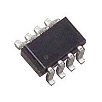
LTC2905CTS8#PBF Linear Technology, LTC2905CTS8#PBF Datasheet - Page 11

LTC2905CTS8#PBF
Manufacturer Part Number
LTC2905CTS8#PBF
Description
Manufacturer
Linear Technology
Datasheet
1.LTC2905CTS8PBF.pdf
(16 pages)
Specifications of LTC2905CTS8#PBF
Voltage Supervisor Type
Voltage Monitor
Number Of Voltage Supervisors
2
Operating Supply Voltage (min)
1V
Package Type
TSOT-23
Operating Temperature Classification
Commercial
Operating Temp Range
0C to 70C
Pin Count
8
Mounting
Surface Mount
Lead Free Status / RoHS Status
Compliant
Available stocks
Company
Part Number
Manufacturer
Quantity
Price
APPLICATIONS INFORMATION
Figure 1 shows the desired delay time as a function of the
value of the timer capacitor that should be used:
Leaving the TMR pin open with no external capacitor gen-
erates a reset time-out of approximately 200μs. For long
reset time-out, the only limitation is the availability of large
value capacitor with low leakage. The TMR capacitor will
never charge if the leakage current exceeds the minimum
TMR charging current of 2.1μA (typical).
RST and RST Output Characteristics
The DC characteristics of the RST and RST pull-up and
pull-down strength are shown in the Typical Performance
Characteristics section. Both RST and RST have a weak
internal pull-up to V
down to ground.
The weak pull-up and strong pull-down arrangement allow
these two pins to have open-drain behavior while possess-
ing several other benefi cial characteristics.
The weak pull-ups eliminate the need for external pull-up
resistors when the rise time on these pins is not critical. On
the other hand, the open-drain RST confi guration allows
for wired-OR connections and can be useful when more
than one signal needs to pull down on the RST line.
Figure 1. Reset Time-Out Period vs Capacitance
10000
1000
100
0.1
10
1
10p
100p
CC
= Max (V1, V2) and a strong pull-
C
TMR
1n
(FARAD)
10n
100n
29045 F01
1μ
As noted in the Power-Up and Power-Down sections the
circuits that drive RST and RST are powered by V
fault condition, V
V
current on RST is barely turned on. Therefore, an external
pull-up resistor of no more than 100k is recommended on
the RST pin if the state and pull-up strength of the RST
pin is crucial at very low V
Note however, by adding an external pull-up resistor, the
pull-up strength on the RST pin is increased. Therefore,
if it is connected in a wired-OR connection, the pull-down
strength of any single device needs to accommodate this
additional pull-up strength.
Output Rise and Fall Time Estimation
The RST and RST outputs have strong pull-down capabil-
ity. The following formula estimates the output fall time
(90% to 10%) for a particular external load capacitance
(C
where R
transistor estimated to be typically 40Ω at room tempera-
ture (25°C) and C
the pin. Assuming a 150pF load capacitance, the fall time
is about 13ns.
The rise time, on the RST and RST pins is limited by weak
internal pull-up current sources to V
formula estimates the output rise time (10% to 90%) at
the RST and RST pins:
where R
Notice that this pull-up transistor is modeled as a
6μA current source in the Block Diagram as a typical
representation.
OL
LOAD
t
t
FALL
RISE
= 0.4V at RST. However, at V
):
≈ 2.2 • R
≈ 2.2 R
PD
PU
is the on-resistance of the internal pull-down
is the on-resistance of the pull-up transistor.
PU
CC
PD
LOAD
• C
of at least 1V guarantees a maximum
• C
LTC2904/LTC2905
LOAD
is the external load capacitance on
LOAD
CC
.
CC
= 1V the weak pull-up
CC
. The following
CC
. During
11
29045fc


