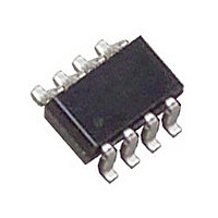
LTC2905CTS8#PBF Linear Technology, LTC2905CTS8#PBF Datasheet - Page 7

LTC2905CTS8#PBF
Manufacturer Part Number
LTC2905CTS8#PBF
Description
Manufacturer
Linear Technology
Datasheet
1.LTC2905CTS8PBF.pdf
(16 pages)
Specifications of LTC2905CTS8#PBF
Voltage Supervisor Type
Voltage Monitor
Number Of Voltage Supervisors
2
Operating Supply Voltage (min)
1V
Package Type
TSOT-23
Operating Temperature Classification
Commercial
Operating Temp Range
0C to 70C
Pin Count
8
Mounting
Surface Mount
Lead Free Status / RoHS Status
Compliant
Available stocks
Company
Part Number
Manufacturer
Quantity
Price
PIN FUNCTIONS
BLOCK DIAGRAM
V2 (Pin 1/Pin 4): Voltage Input 2. Input for V2 monitor.
Select from 3.3V, 2.5V, 1.8V, 1.5V, 1.2V or 1.0V. Refer to
Table 1 for details. The greater of V1, V2 is also the internal
supply voltage, V
(or greater) capacitor.
RST (Pin 2/Pin 3): (LTC2904 Only) Reset Logic Output.
When all voltage inputs are above the reset threshold for
at least the programmed delay time, this pin pulls low. This
pin has a weak pull-up to V
V
TMR (Pin 2/Pin 3): (LTC2905 Only) Reset Delay Time
Programming Pin. Attach an external capacitor (C
GND to set a reset delay time of 9ms/nF . Leaving the pin
open generates a minimum delay of approximately 200μs. A
22nF capacitor will generate a 200ms reset delay time.
RST (Pin 3/Pin 2): Inverted Reset Logic Output. Pulls low
when any voltage input is below the reset threshold and is
held low for programmed delay time after all voltage inputs
CC
using an external pull-up.
V1
V2
CC
. Bypass this pin to ground with a 0.1μF
LTC2904
REFERENCE
BAND GAP
POWER
DETECT
(TS8 Package/DDB8 Package)
CC
and may be pulled above
V
CC
RESISTOR
NETWORK
–
+
–
+
TMR
S1
) to
THREE-STATE DECODER
are above threshold. This pin has a weak pull-up to V
and may be pulled above V
GND (Pin 4/Pin 1, Pin 9): Ground.
TOL (Pin 5/Pin 8): Three-state Input for Supply Tolerance
Selection (5%, 7.5% or 10%). See the Applications Infor-
mation section for tolerance selection chart (Table 2).
S1 (Pin 6/Pin 7): Voltage Threshold Select Three-State
Input. Connect to V1, GND or leave unconnected in open
state (See Table 1).
S2 (Pin 7/Pin 6): The Second Voltage Threshold Select
Three-State Input. Connect to V1, GND or leave uncon-
nected in open state (See Table 1).
V1 (Pin 8/Pin 5): Voltage Input 1. Input for V1 monitor.
Select from 5V, 3.3V, or 2.5V. See Table 1 for details.
The greater of V1, V2 is also the internal supply voltage,
V
capacitor.
CC
. Bypass this pin to ground with a 0.1μF (or greater)
S2
RESET PULSE
GENERATOR
200ms
TOL
LTC2904/LTC2905
6μA
6μA
CC
V
V
using an external pull-up.
CC
CC
2904 BD
RST
RST
GND
29045fc
7
CC


