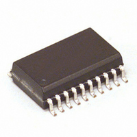
MC88LV926DWR2 Freescale Semiconductor, MC88LV926DWR2 Datasheet - Page 2

MC88LV926DWR2
Manufacturer Part Number
MC88LV926DWR2
Description
IC DRIVER CLK PLL 66MHZ 20-SOIC
Manufacturer
Freescale Semiconductor
Type
PLL Clock Driverr
Datasheet
1.MC88LV926DWR2.pdf
(12 pages)
Specifications of MC88LV926DWR2
Input
CMOS, TTL
Output
CMOS
Frequency - Max
66MHz
Voltage - Supply
3 V ~ 3.6 V
Operating Temperature
0°C ~ 70°C
Mounting Type
Surface Mount
Package / Case
20-SOIC (7.5mm Width)
Frequency-max
66MHz
Lead Free Status / RoHS Status
Contains lead / RoHS non-compliant
Other names
MC88LV926DWR2TR
Available stocks
Company
Part Number
Manufacturer
Quantity
Price
MC88LV926
Description of the RST_IN/RST_OUT(LOCK) Functionality (continued)
phase–locked to the SYNC input signal (RST_OUT high), the
processor reset functionality can be utilized. When the
RST_IN pin is toggled low (min. pulse width=10nS),
RST_OUT(LOCK) will go to the low state and remain there
for 1024 cycles of the ‘Q’ output frequency (512 SYNC
cycles). During the time in which the RST_OUT(LOCK) is
actively pulled low, all the 88LV926 clock outputs will
continue operating correctly and in a locked condition to the
SYNC input (clock signals to the 68030/040/060 family of
processors must continue while the processor is in reset). A
propagation delay after the 1024th cycle RST_OUT(LOCK)
goes back to the high impedance state to be pulled high by
the resistor.
Power Supply Ramp Rate Restriction for Correct 030/040
Processor Reset Operation During System Start–up
CAPACITANCE AND POWER SPECIFICATIONS
* Value at V CC = 3.3V TBD.
C IN
C PD
PD 1
PD 2
MOTOROLA
After the system start–up is complete and the 88LV926 is
Symbol
Because the RST_OUT(LOCK) pin is an indicator of
Input Capacitance
Power Dissipation Capacitance
Power Dissipation at 33MHz With 50
Thevenin Termination
Power Dissipation at 33MHz With 50
Parallel Termination to GND
Parameter
Pinout: 20–Lead Wide SOIC Package (Top View)
GND(AN)
V CC (AN)
RST_IN
SYNC
GND
V CC
RC1
MR
Q3
Q0
10
1
2
3
4
5
6
7
8
9
37.5mW/Output*
225mW/Device
15mW/Output*
90mW/Device
Value Typ
2
4.5*
40*
phase–lock to the reference source, some constraints must
be placed on the power supply ramp rate to make sure the
RST_OUT(LOCK) signal holds the processor in reset during
system start–up (power–up). With the recommended loop
filter values (see Figure 6.) the lock time is approximately
10ms. The phase–lock loop will begin attempting to lock to a
reference source (if it is present) when VCC reaches 2V. If
the V CC ramp rate is significantly slower than 10ms, then the
PLL could lock to the reference source, causing
RST_OUT(LOCK) to go high before the 88LV926 and
’030/040 processor is fully powered up, violating the
processor reset specification. Therefore, if it is necessary for
the RST_IN pin to be held high during power–up, the V CC
ramp rate must be less than 10mS for proper 68030/040/060
reset operation.
can be held low during system start–up (which holds
RST_OUT low). The RST_OUT(LOCK) pin will then be
pulled back high 1024 cycles after the RST_IN pin goes high.
This ramp rate restriction can be ignored if the RST_IN pin
20
19
18
17
16
15
14
13
12
11
GND
2X_Q
QCLKEN
V CC
Q2
GND
RST_OUT(LOCK)
PLL_EN
Q1
V CC
Unit
mW
mW
pF
pF
Test Conditions
V CC = 5.0V
V CC = 5.0V
V CC = 5.0V
V CC = 5.0V
T = 25 C
T = 25 C
TIMING SOLUTIONS


