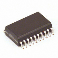
MC88LV926DWR2 Freescale Semiconductor, MC88LV926DWR2 Datasheet - Page 5

MC88LV926DWR2
Manufacturer Part Number
MC88LV926DWR2
Description
IC DRIVER CLK PLL 66MHZ 20-SOIC
Manufacturer
Freescale Semiconductor
Type
PLL Clock Driverr
Datasheet
1.MC88LV926DWR2.pdf
(12 pages)
Specifications of MC88LV926DWR2
Input
CMOS, TTL
Output
CMOS
Frequency - Max
66MHz
Voltage - Supply
3 V ~ 3.6 V
Operating Temperature
0°C ~ 70°C
Mounting Type
Surface Mount
Package / Case
20-SOIC (7.5mm Width)
Frequency-max
66MHz
Lead Free Status / RoHS Status
Contains lead / RoHS non-compliant
Other names
MC88LV926DWR2TR
Available stocks
Company
Part Number
Manufacturer
Quantity
Price
AC CHARACTERISTICS (T A = 0 C to 70 C; V CC = 3.3V
1. These specifications are not tested, they are guaranteed by statistical characterization. See Application Note 1 for a discussion of this
2. Under equally loaded conditions and at a fixed temperature and voltage.
3. With V CC fully powered–on: t CLOCK Max is with C1 = 0.1 F; t LOCK Min is with C1 = 0.01 F.
4. See Application Note 4 for the distribution in time of each output referenced to SYNC.
5. Specification is valid only when the PLL_EN pin is low.
6. Guaranteed that QCLKEN will meet the setup and hold time requirement of the 68060.
TIMING SOLUTIONS
t RISE/FALL
All Outputs
t RISE/FALL
2X_Q Output
t pulse width(a) 1
(Q0, Q1, Q2, Q3)
t pulse width(b) 1
(2X_Q Output)
t SKEWr 2
(Rising)
t SKEWf 2
(Falling)
t SKEWall 2
t SKEW QCLKEN 1,2
t LOCK 3
t PHL MR – Q 1
t REC , MR to SYNC 5,
1
t W , MR LOW 5, 1
t W , RST_IN LOW 1
t PZL 1
t PLZ 1
methodology.
Symbol
Rise/Fall Time, into 50 Load
Rise/Fall Time into a 50 Load
Output Pulse Width
Q0, Q1, Q2, Q3 at 1.65V
Output Pulse Width
2X_Q at 1.65V
Output–to–Output Skew
Between Outputs Q0–Q2
(Rising Edge Only)
Output–to–Output Skew
Between Outputs Q0–Q2
(Falling Edge Only)
Output–to–Output Skew
2X_Q, Q0–Q2, Q3
Output–to–Output Skew
QCLKEN to 2X_Q
Phase–Lock Acquisition Time,
All Outputs to SYNC Input
Propagation Delay,
MR to Any Output (High–Low)
Reset Recovery Time rising MR edge to
falling SYNC edge
Minimum Pulse Width, MR input Low
Minimum Pulse Width, RST_IN Low
Output Enable Time
RST_IN Low to RST_OUT Low
Output Enable Time
RST_IN High to RST_OUT High Z
Parameter
2X_Q = 50MHz
2X_Q = 66MHz
0.3V or 5.0V 5%)
(508 Q/2 Cycles)
1016 ‘Q’ Cycles
0.5t cycle – 0.5
0.5t cycle – 0.5
5
Mimimum
9.7 6
7.0 6
0.3
0.5
1.5
1.5
—
—
—
10
1
9
5
(512 Q/2 Cycles)
1024 ‘Q’ Cycles
0.5t cycle + 0.5
0.5t cycle + 0.5
Maximum
13.5
16.5
500
750
1.6
1.6
1.0
10
—
—
—
—
Unit
ms
ns
ns
ns
ns
ps
ns
ps
ns
ns
ns
ns
ns
ns
ns
t RISE – 0.8V to 2.0V
t FALL – 2.0V to 0.8V
t RISE – 0.8V to 2.0V
t FALL – 2.0V to 0.8V
50 Load Terminated to
V CC /2 (See Application
Note 3)
50 Load Terminated to
V CC /2 (See Application
Note 3)
Into a 50 Load
Terminated to V CC /2
(See Timing Diagram in
Figure 5.)
Into a 50 Load
Terminated to V CC /2
(See Timing Diagram in
Figure 5.)
Into a 50 Load
Terminated to V CC /2
(See Timing Diagram in
Figure 5.)
Into a 50 Load
Terminated to V CC /2
(See Timing Diagram in
Figure 5.)
Into a 50 Load
Terminated to V CC /2
When in Phase–Lock
See Application
Note 5
See Application
Note 5
Condition
MC88LV926
MOTOROLA


