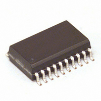
MC88LV926DWR2 Freescale Semiconductor, MC88LV926DWR2 Datasheet - Page 6

MC88LV926DWR2
Manufacturer Part Number
MC88LV926DWR2
Description
IC DRIVER CLK PLL 66MHZ 20-SOIC
Manufacturer
Freescale Semiconductor
Type
PLL Clock Driverr
Datasheet
1.MC88LV926DWR2.pdf
(12 pages)
Specifications of MC88LV926DWR2
Input
CMOS, TTL
Output
CMOS
Frequency - Max
66MHz
Voltage - Supply
3 V ~ 3.6 V
Operating Temperature
0°C ~ 70°C
Mounting Type
Surface Mount
Package / Case
20-SOIC (7.5mm Width)
Frequency-max
66MHz
Lead Free Status / RoHS Status
Contains lead / RoHS non-compliant
Other names
MC88LV926DWR2TR
Available stocks
Company
Part Number
Manufacturer
Quantity
Price
MC88LV926
1. Several specifications can only be measured when the
MOTOROLA
MC88LV926 is in phase–locked operation. It is not
possible to have the part in phase–lock on ATE
(automated test equipment). Statistical characterization
techniques were used to guarantee those specifications
which cannot be measured on the ATE. MC88LV926 units
were fabricated with key transistor properties intentionally
varied to create a 14 cell designed experimental matrix. IC
performance was characterized over a range of transistor
properties (represented by the 14 cells) in excess of the
expected process variation of the wafer fabrication area.
Response Surface Modeling (RSM) techniques were
used to relate IC performance to the CMOS transistor
properties over operation voltage and temperature. IC
performance to each specification and fab variation were
used in conjunction with Yield Surface Modeling
(YSM ) methodology to set performance limits of ATE
testable specifications within those which are to be
guaranteed by statistical characterization. In this way, all
units passing the ATE test will meet or exceed the
non–tested specifications limits.
LOOP FILTER
WITH THE 470K RESISTOR TIED IN THIS FASHION THE T PD
SPECIFICATION, MEASURED AT THE INPUT PINS IS:
EXTERNAL
SYNC INPUT
Q0 OUTPUT
t PD = 2.25ns 1.0ns (TYPICAL VALUES)
Figure 2. Depiction of the Fixed SYNC to Q0 Offset (t PD ) Which Is Present
0.1 F
OFFSET
2.25ns
330
RC1
ANALOG GND
R2
C1
When a 470K Resistor Is Tied to V CC or Ground
3V
470K
REFERENCE
RESISTOR
5V
Application Notes
6
2. A 470K
3. Two specs (t RISE/FALL and t PULSE Width 2X_Q output,
GND, as shown in Figure 2., is required to ensure no jitter
is present on the MC88LV926 outputs. This technique
causes a phase offset between the SYNC input and the
Q0 output, measured at the pins. The t PD spec describes
how this offset varies with process, temperature, and
voltage. The specs were arrived at by measuring the
phase relationship for the 14 lots described in note 1 while
the part was in phase–locked operation. The actual
measurements were made with a 10MHz SYNC input
(1.0ns edge rate from 0.8V to 2.0V). The phase
measurements were made at 1.5V. See Figure 2. for a
graphical description.
see AC Specifications) guarantee that the MC88LV926
meets the 33MHz and 66MHz 68060 P–Clock input
specification.
WITH THE 470K RESISTOR TIED IN THIS FASHION THE T PD
SPECIFICATION, MEASURED AT THE INPUT PINS IS:
SYNC INPUT
Q0 OUTPUT
resistor tied to either Analog V CC or Analog
REFERENCE
RESISTOR
t PD = –0.80ns 0.30ns
470K
ANALOG V CC
ANALOG GND
OFFSET
–0.8ns
0.1 F
330
RC1
TIMING SOLUTIONS
R2
C1
5V
3V


