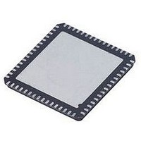
AD9548BCPZ Analog Devices Inc, AD9548BCPZ Datasheet - Page 31

AD9548BCPZ
Manufacturer Part Number
AD9548BCPZ
Description
IC CLOCK GEN/SYNCHRONIZR 88LFCSP
Manufacturer
Analog Devices Inc
Datasheet
1.AD9548BCPZ-REEL7.pdf
(112 pages)
Specifications of AD9548BCPZ
Input
*
Output
*
Frequency - Max
*
Voltage - Supply
*
Operating Temperature
*
Mounting Type
Surface Mount
Package / Case
88-LFCSP
Frequency-max
*
Clock Ic Type
Clock Synthesizer
Ic Interface Type
Serial
Frequency
1GHz
No. Of Outputs
4
No. Of Multipliers / Dividers
4
Supply Current
190mA
Lead Free Status / RoHS Status
Lead free / RoHS Compliant
Available stocks
Company
Part Number
Manufacturer
Quantity
Price
Part Number:
AD9548BCPZ
Manufacturer:
ADI/亚德诺
Quantity:
20 000
Company:
Part Number:
AD9548BCPZ-SMD7
Manufacturer:
SHARP
Quantity:
392
Phase Build-Out Reference Switching
Phase build-out reference switching is the term given to a
reference switchover that completely masks any phase
difference between the previous reference and the new
reference. That is, there is virtually no phase change detectable
at the output when a phase build-out switchover occurs.
The AD9548 handles phase build-out switching based on
whether the new reference is a phase master. A phase master is
any reference with a selection priority value that is less than the
phase master threshold priority value (that is, higher priority).
The phase master threshold priority value resides in the phase
build-out switching register (Address 0507), whereas the
selection priority resides in the profile registers (Address 0600
to Address 07FF). By default, the phase master threshold
priority is 0; therefore, no references can be phase masters until
the user changes the phase master threshold priority.
Whenever the AD9548 switches from one reference to another,
it compares the selection priority value stored in the profile
assigned to the new reference with the phase master threshold
priority. The AD9548 performs a phase build-out switchover
only if the new reference is not a phase master.
Hitless Reference Switching (Phase Slew Control)
Hitless reference switching is the term given to a reference
switchover that limits the rate of change of the phase of the
output clock while the PLL is in the process of acquiring phase
lock. This prevents the output frequency offset from becoming
excessive.
C/CC
D/DD
A/AA
B/BB
SELECTION
PROFILE
INPUT
A
B
C
D
PRIORITY TABLE
COMMON
WITHOUT PROMOTION
WITH PROMOTION
PRIORITY
0
1
2
3
MONITORS
PROMOTED
0
0
1
2
Figure 36. Reference Clock Block Diagram
Figure 35. Example of Priority Promotion
INITIAL
STATE
VALIDATION
Rev. A | Page 31 of 112
LOGIC
ALL VALID
A VALID
B VALID
The all-digital nature of the DPLL core (see the Digital PLL
(DPLL) Core section) gives the user numerical control of the
rate at which phase changes occur at the DPLL output. When
enabled, a phase slew controller monitors the phase difference
between the feedback and reference inputs to the DPLL. The
phase slew controller has the ability to place a user-specified
limit on the rate of change of phase, thus providing a
mechanism for hitless reference switching.
The user sets a limit on the rate of change of phase by storing
the appropriate value in the 16-bit phase slew rate limit register
(Address 0316 to Address 0317). The 16-bit word (representing
ns/sec) puts an upper bound on the rate of change of the phase
at the output of the DPLL during a reference switchover. A
phase slew rate value of 0 (default) disables the phase slew
controller.
The accuracy of the phase slew controller depends on both the
phase slew limit value and the system clock frequency.
Generally, an increase in the phase slew rate limit value or a
decrease in the system clock frequency tends to reduce the
error. As such, the accuracy is best for the largest phase slew
limit value and the lowest system clock frequency. For example,
assuming the use of a 1 GHz system clock, a phase slew limit
value of 315 ns/sec (or more) ensures an error of less than 10%,
whereas a phase slew rate limit value above ~3100 ns/sec
ensures an error of less than 1%. On the other hand, assuming
the use of a 500 MHz system clock, the same phase slew rate
limit values ensure an error of less than 5% or 0.5%,
respectively.
A FAULTED
SELECTION
B FAULTED
PRIORITY
ACTIVE
ACTIVE
ACTIVE
A
B
C
B VALID
CONTROLLER
A VALID
LOOP
÷R
TDC
AD9548


