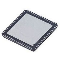
AD9548BCPZ Analog Devices Inc, AD9548BCPZ Datasheet - Page 78

AD9548BCPZ
Manufacturer Part Number
AD9548BCPZ
Description
IC CLOCK GEN/SYNCHRONIZR 88LFCSP
Manufacturer
Analog Devices Inc
Datasheet
1.AD9548BCPZ-REEL7.pdf
(112 pages)
Specifications of AD9548BCPZ
Input
*
Output
*
Frequency - Max
*
Voltage - Supply
*
Operating Temperature
*
Mounting Type
Surface Mount
Package / Case
88-LFCSP
Frequency-max
*
Clock Ic Type
Clock Synthesizer
Ic Interface Type
Serial
Frequency
1GHz
No. Of Outputs
4
No. Of Multipliers / Dividers
4
Supply Current
190mA
Lead Free Status / RoHS Status
Lead free / RoHS Compliant
Available stocks
Company
Part Number
Manufacturer
Quantity
Price
Part Number:
AD9548BCPZ
Manufacturer:
ADI/亚德诺
Quantity:
20 000
Company:
Part Number:
AD9548BCPZ-SMD7
Manufacturer:
SHARP
Quantity:
392
AD9548
Table 67. Distribution Synchronization
Address
0402
Table 68. Automatic Synchronization
Address
0403
Table 69. Distribution Channel Modes
Address
0404
Bits
[7:6]
[5:4]
[3]
[2]
[1]
[0]
Bits
[7:2]
[1:0]
Bits
[7:6]
[5]
[4]
[3]
[2:0]
Bit Name
Unused
Sync source
OUT3 sync mask
OUT2 sync mask
OUT1 sync mask
OUT0 sync mask
Bit Name
Unused
Automatic sync mode
Bit Name
Unused
OUT0 CMOS phase
invert
OUT0 polarity invert
OUT0 drive strength
OUT0 mode
00 (default) = direct.
01 = active reference.
10 = DPLL feedback edge.
11 = reserved.
0 (default) = unmasked
1 = masked.
0 (default) = unmasked.
1 = masked.
0 (default) = unmasked.
1 = masked.
0 (default) = unmasked.
1 = masked.
Description
Select the sync source for the clock distribution output channels.
Mask the synchronous reset to the OUT3 divider.
Mask the synchronous reset to the OUT2 divider.
Mask the synchronous reset to the OUT1 divider.
Mask the synchronous reset to the OUT0 divider.
Description
When the output mode is CMOS, the bit inverts the relative phase between the two
CMOS output pins. Otherwise, this bit is nonfunctional.
0 (default) = not inverted.
1 = inverted.
Invert the polarity of OUT0.
0 (default) = not inverted.
1 = inverted.
OUT0 output drive capability control.
0 (default) = CMOS: low drive strength; LVDS: 3.5 mA nominal.
1 = CMOS: normal drive strength; LVDS: 7 mA nominal.
OUT0 operating mode select.
000 = CMOS (both pins)
001 = CMOS (positive pin), tristate (negative pin).
010 = tristate (positive pin), CMOS (negative pin).
011 (default) = tristate (both pins).
100 = LVDS.
101 = LVPECL.
110 = reserved.
111 = reserved.
Description
Autosync mode
00 (default) = disabled
01 = sync on DPLL frequency lock
10 = sync on DPLL phase lock
11 = reserved
Rev. A | Page 78 of 112


