PCKV857ADGG,518 NXP Semiconductors, PCKV857ADGG,518 Datasheet - Page 2
PCKV857ADGG,518
Manufacturer Part Number
PCKV857ADGG,518
Description
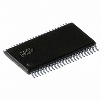
IC 1:10 2.5V PLL CLK-DRVR48TSSOP
Manufacturer
NXP Semiconductors
Type
PLL Clock Driverr
Datasheet
1.PCKV857ADGG512.pdf
(13 pages)
Specifications of PCKV857ADGG,518
Input
SSTL-2
Output
SSTL-2
Frequency - Max
250MHz
Voltage - Supply
2.375 V ~ 2.625 V
Operating Temperature
0°C ~ 70°C
Mounting Type
Surface Mount
Package / Case
48-TSSOP
Frequency-max
250MHz
Lead Free Status / RoHS Status
Lead free / RoHS Compliant
Other names
935272504518
PCKV857ADGG-T
PCKV857ADGG-T
PCKV857ADGG-T
PCKV857ADGG-T


FEATURES
•
•
•
•
•
•
•
•
•
•
•
•
•
•
DESCRIPTION
The PCKV857A is a high-performance, low-skew, low-jitter zero
delay buffer designed for 2.5 V V
differential data input and output levels.
The PCKV857A is a zero delay buffer that distributes a differential
clock input pair (CLK, CLK) to ten differential pairs of clock outputs
(Y[0:9], Y[0:9]) and one differential pair feedback clock outputs
(FB
inputs (CLK, CLK), the feedback clocks (FB
power input (AV
phase and frequency with CLK. When PWRDWN is LOW, all
outputs are disabled to HIGH impedance state (3-State), and the
PLL is shut down (LOW power mode). The device also enters the
LOW power mode when the input frequency falls below 20 MHz. An
input frequency detection circuit will detect the LOW frequency
condition and after applying a > 20 MHz input signal, the detection
circuit turns on the PLL again and enables the outputs.
When AV
purposes. The PCKV857A is also able to track spread spectrum
clocking for reduced EMI.
The PCKV857A is characterized for operation from 0 to +70 °C.
ORDERING INFORMATION
Philips Semiconductors
2003 Jul 31
ESD classification testing is done to JEDEC Standard JESD22.
Protection exceeds 2000 V to HBM per method A114.
Latch-up testing is done to JEDEC Standard JESD78 which
exceeds 100 mA
Optimized for clock distribution in DDR (Double Data Rate)
SDRAM applications as per JEDEC specifications
1-to-10 differential clock distribution
Very low skew (< 100 ps) and jitter (< 100 ps)
Operation from 2.2 V to 2.7 V AV
SSTL_2 interface clock inputs and outputs
CMOS control signal input
Test mode enables buffers while disabling PLL
Low current power-down mode
Tolerant of Spread Spectrum input clock
Full DDR solution provided when used with SSTL16877 or
SSTV16857
Designed for DDR 266, 300, and 333 DIMM applications
Available in TSSOP-48 and TVSOP-48 packages
100-250 MHz differential 1:10 clock driver
48-Pin Plastic TSSOP (TVSOP)
OUT
, FB
48-Pin Plastic TSSOP
DD
OUT
PACKAGES
is grounded, the PLL is turned off and bypassed for test
) . The clock outputs are controlled by the clock
DD
). When PWRDWN is HIGH, the outputs switch in
DD
DD
and 2.5 V AV
and 2.3 V to 2.7 V V
TEMPERATURE RANGE
IN
, FB
DD
IN
0 to +70 °C
0 to +70 °C
), and the analog
operation and
DD
2
PIN CONFIGURATION
PCKV857ADGG
PCKV857ADGV
ORDER CODE
AGND
V
V
V
V
V
AV
GND
GND
GND
GND
GND
DDQ
DDQ
DDQ
CLK
CLK
DDQ
DDQ
Y
Y
Y
Y
Y
Y
DD
Y
Y
Y
Y
0
0
1
1
2
2
3
3
4
4
10
11
12
13
14
15
16
17
18
19
21
22
23
24
7
20
1
2
3
4
5
6
8
9
48
47
46
45
44
43
42
41
40
39
38
37
36
35
34
33
32
31
30
29
28
27
25
26
DRAWING NUMBER
GND
Y
Y
V
Y
Y
GND
GND
Y
Y
V
PWRDWN
FB
FB
V
FB
FB
GND
Y
Y
V
Y
Y
GND
5
5
DDQ
6
6
7
7
DDQ
DDQ
8
8
DDQ
9
9
SW00691
IN
IN
OUT
OUT
PCKV857A
SOT362-1
SOT480-1
Product data
Related parts for PCKV857ADGG,518
Image
Part Number
Description
Manufacturer
Datasheet
Request
R

Part Number:
Description:
Manufacturer:
NXP Semiconductors
Datasheet:
Part Number:
Description:
NXP Semiconductors designed the LPC2420/2460 microcontroller around a 16-bit/32-bitARM7TDMI-S CPU core with real-time debug interfaces that include both JTAG andembedded trace
Manufacturer:
NXP Semiconductors
Datasheet:

Part Number:
Description:
NXP Semiconductors designed the LPC2458 microcontroller around a 16-bit/32-bitARM7TDMI-S CPU core with real-time debug interfaces that include both JTAG andembedded trace
Manufacturer:
NXP Semiconductors
Datasheet:
Part Number:
Description:
NXP Semiconductors designed the LPC2468 microcontroller around a 16-bit/32-bitARM7TDMI-S CPU core with real-time debug interfaces that include both JTAG andembedded trace
Manufacturer:
NXP Semiconductors
Datasheet:
Part Number:
Description:
NXP Semiconductors designed the LPC2470 microcontroller, powered by theARM7TDMI-S core, to be a highly integrated microcontroller for a wide range ofapplications that require advanced communications and high quality graphic displays
Manufacturer:
NXP Semiconductors
Datasheet:
Part Number:
Description:
NXP Semiconductors designed the LPC2478 microcontroller, powered by theARM7TDMI-S core, to be a highly integrated microcontroller for a wide range ofapplications that require advanced communications and high quality graphic displays
Manufacturer:
NXP Semiconductors
Datasheet:
Part Number:
Description:
The Philips Semiconductors XA (eXtended Architecture) family of 16-bit single-chip microcontrollers is powerful enough to easily handle the requirements of high performance embedded applications, yet inexpensive enough to compete in the market for hi
Manufacturer:
NXP Semiconductors
Datasheet:
Part Number:
Description:
The XA-S3 device is a member of Philips Semiconductors? XA(eXtended Architecture) family of high performance 16-bitsingle-chip microcontrollers
Manufacturer:
NXP Semiconductors
Datasheet:

Part Number:
Description:
The NXP BlueStreak LH75401/LH75411 family consists of two low-cost 16/32-bit System-on-Chip (SoC) devices
Manufacturer:
NXP Semiconductors
Datasheet:
Part Number:
Description:
The NXP LPC3130/3131 combine an 180 MHz ARM926EJ-S CPU core, high-speed USB2
Manufacturer:
NXP Semiconductors
Datasheet:
Part Number:
Description:
The NXP LPC3141 combine a 270 MHz ARM926EJ-S CPU core, High-speed USB 2
Manufacturer:
NXP Semiconductors
Part Number:
Description:
The NXP LPC3143 combine a 270 MHz ARM926EJ-S CPU core, High-speed USB 2
Manufacturer:
NXP Semiconductors

Part Number:
Description:
The NXP LPC3152 combines an 180 MHz ARM926EJ-S CPU core, High-speed USB 2
Manufacturer:
NXP Semiconductors
Part Number:
Description:
The NXP LPC3154 combines an 180 MHz ARM926EJ-S CPU core, High-speed USB 2
Manufacturer:
NXP Semiconductors