MC100ES6226AC IDT, Integrated Device Technology Inc, MC100ES6226AC Datasheet - Page 5
MC100ES6226AC
Manufacturer Part Number
MC100ES6226AC
Description
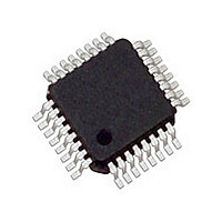
IC CLK DIVIDER FAN BUFF 32LQFP
Manufacturer
IDT, Integrated Device Technology Inc
Type
Fanout Buffer (Distribution), Dividerr
Series
100ESr
Datasheet
1.MC100ES6226AC.pdf
(9 pages)
Specifications of MC100ES6226AC
Number Of Circuits
1
Ratio - Input:output
1:9
Differential - Input:output
Yes/Yes
Input
LVCMOS, LVPECL
Output
LVPECL
Frequency - Max
3GHz
Voltage - Supply
2.375 V ~ 3.465 V
Operating Temperature
0°C ~ 110°C
Mounting Type
Surface Mount
Package / Case
32-LQFP
Frequency-max
3GHz
Number Of Clock Inputs
1
Mode Of Operation
Differential
Output Frequency
3000MHz
Output Logic Level
LVPECL
Operating Supply Voltage (min)
2.375V
Operating Supply Voltage (typ)
2.5/3.3V
Operating Supply Voltage (max)
3.465V
Package Type
TQFP
Operating Temp Range
0C to 110C
Operating Temperature Classification
Commercial
Signal Type
LVPECL
Mounting
Surface Mount
Pin Count
32
Lead Free Status / RoHS Status
Lead free / RoHS Compliant
Other names
800-2002
MC100ES6226ACIDT
MC100ES6226ACIDT
Available stocks
Company
Part Number
Manufacturer
Quantity
Price
Company:

Part Number:
MC100ES6226AC
Manufacturer:
ON
Quantity:
184
Company:
Part Number:
MC100ES6226AC
Manufacturer:
IDT, Integrated Device Technology Inc
Quantity:
10 000
Company:
Part Number:
MC100ES6226ACR2
Manufacturer:
IDT, Integrated Device Technology Inc
Quantity:
10 000


Table 6. DC Characteristics (V
IDT™ / ICS™ CLOCK DISTRIBUTION BUFFER/CLOCK DRIVER
LVCMOS Control Inputs (OE, FSEL0, FSEL1, MR)
LVPECL Clock Inputs (CLK, CLK)
LVPECL Clock Outputs (QA[2:0], QB[2:0], QC[2:0])
Supply Current
Symbol
1. AC characteristics are design targets and pending characterization.
2. Input have internal pullup/pulldown resistors which affect the input current.
3. Clock inputs driven by LVPECL compatible signals.
4. V
5. V
MC100ES6226
2.5V/3.3V DIFFERENTIAL LVPECL 1:9 CLOCK DISTRIBUTION BUFFER AND CLOCK DRIVER
V
I
V
V
V
V
V
GND
V
V
I
CMR
I
I
CC
range and the input swing lies within the V
IN
IN
OH
PP
OL
IH
IH
IL
IL
PP
CMR
is the minimum differential input voltage swing required to maintain AC characteristic.
(DC) is the crosspoint of the differential input signal. Functional operation is obtained when the crosspoint is within the V
Input Voltage Low
Input Voltage High
Input Current
DC Differential Input Voltage
Differential Cross Point Voltage
Input High Voltage
Input Low Voltage
Input Current
Output High Voltage
Output Low Voltage
Maximum Quiescent Supply Current without
Output Termination Current
Maximum Quiescent Supply Current with
Output Termination Current
(2)
Characteristics
(3)
CC
= 3.3 V ± 5% and 2.5 V ± 5%, T
(4)
(5)
V
V
V
V
CC
CC
CC
CC
PP
= 3.3 V
= 2.5 V
= 3.3 V
= 2.5 V
(DC) specification.
V
V
CC
CC
TBD
TBD
Min
2.2
1.7
0.1
1.0
– 1.1
– 1.8
J
5
Typ
325
= 0°C to +110°C)
65
V
V
V
CC
CC
CC
±150
±150
Max
TBD
TBD
110
400
0.8
0.7
1.3
– 0.3
– 0.8
– 1.4
(1)
Unit
mA
mA
µA
µA
V
V
V
V
V
V
MC100ES6226 REV. 5 NOVEMBER 10, 2008
V
Differential operation
Differential operation
V
Termination 50 Ω to V
Termination 50 Ω to V
GND pin
All V
IN
IN
= V
= TBD or V
CC
CC
pins
Condition
or V
IN
IN
= GND
= TBD
CMR
TT
TT
(DC)
Related parts for MC100ES6226AC
Image
Part Number
Description
Manufacturer
Datasheet
Request
R

Part Number:
Description:
MICROCOUPLER, SMALL TRANSISTOR OUTPUT
Manufacturer:
Micropac Industries, Inc.
Part Number:
Description:
Steckbare Anschlussklemmen, Raster 5,08 mm
Manufacturer:
LUMBERG [Lumberg]
Datasheet:

Part Number:
Description:
MC100-50805K
Manufacturer:
Cooper/Bussmann
Datasheet:

Part Number:
Description:
TRANSLATION DEVICE DPI 80-PQFP
Manufacturer:
IDT, Integrated Device Technology Inc
Datasheet:
Part Number:
Description:
IDT PART
Manufacturer:
IDT, Integrated Device Technology Inc
Datasheet:
Part Number:
Description:
IC LIU T1/E1/J1 OCTAL 256PBGA
Manufacturer:
IDT, Integrated Device Technology Inc
Datasheet:

Part Number:
Description:
IC FREQ TIMING GENERATOR 28TSSOP
Manufacturer:
IDT, Integrated Device Technology Inc
Datasheet:
Part Number:
Description:
IC CLK DVR PLL 1:10 40VFQFPN
Manufacturer:
IDT, Integrated Device Technology Inc
Datasheet:
Part Number:
Description:
IC CLK FANOUT BUFFER 1:18 32LQFP
Manufacturer:
IDT, Integrated Device Technology Inc
Datasheet:
Part Number:
Description:
IC CLK FANOUT BUFFER 1:18 32LQFP
Manufacturer:
IDT, Integrated Device Technology Inc
Datasheet: