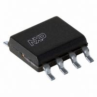
PCK2002PD,112 NXP Semiconductors, PCK2002PD,112 Datasheet - Page 5

PCK2002PD,112
Manufacturer Part Number
PCK2002PD,112
Description
IC PCI-X CLOCK BUFF 533MHZ 8SOIC
Manufacturer
NXP Semiconductors
Type
Fanout Buffer (Distribution)r
Datasheet
1.PCK2002PD112.pdf
(9 pages)
Specifications of PCK2002PD,112
Package / Case
8-SOIC (3.9mm Width)
Number Of Circuits
1
Ratio - Input:output
1:4
Differential - Input:output
No/No
Input
LVTTL
Output
LVTTL
Frequency - Max
533MHz
Voltage - Supply
3 V ~ 3.6 V
Operating Temperature
-40°C ~ 85°C
Mounting Type
Surface Mount
Frequency-max
533MHz
Number Of Outputs
4
Propagation Delay (max)
2.9 ns
Supply Voltage (max)
3.6 V
Supply Voltage (min)
3 V
Maximum Power Dissipation
850 mW
Maximum Operating Temperature
+ 85 C
Minimum Operating Temperature
- 40 C
Mounting Style
SMD/SMT
Lead Free Status / RoHS Status
Lead free / RoHS Compliant
Other names
935269303112
PCK2002PD
PCK2002PD
PCK2002PD
PCK2002PD
Philips Semiconductors
AC CHARACTERISTICS
NOTES:
1. CLK skew is only valid for equal loading of all outputs.
2. t
3. t
4. t
5. Input edge rate for these tests must be faster than 1 V/ns.
6. All typical values are at V
AC WAVEFORMS
V
C
V
output load.
2002 Dec 13
M
OL
L
533 MHz PCI-X clock buffer
= 25 pF
= 50% V
SYMBOL
SYMBOL
H
L
R
and V
t
BUF_OUT
DDSKW
is measured at 0.35 V
is measured at 0.5 V
and t
t
t
t
SKW
PLH
PHL
t
t
t
t
BUF_IN
t
t
H
H
R
L
L
F
0.35 V
INPUT
0.5 V
0.4 V
OH
Figure 1. Load circuitry for switching times.
F
DD
are measured as a transition through the threshold region 0.2 V
DD
DD
DD
are the typical output voltage drop that occur with the
0.6 V
0.2 V
Figure 2. Buffer Output clock
CLK HIGH time
CLK LOW time
CLK HIGH time
CLK LOW time
Output rise slew rate
Output fall slew rate
Buffer LH propagation delay
Buffer HL propagation delay
Bus CLK skew
Device to device skew
DD
DD
V
T
M
t
DD
R
t
PLH
h
DD
CC
V
as shown in Figure 2.
M
PARAMETER
PARAMETER
as shown in Figure 2.
= 3.3 V and T
t
p
V
M
V
t
l
DD
t
PHL
amb
= 25 °C.
SW00812
V
M
T
F
SW00811
0.6 V
0.2 V
DD
DD
TEST CONDITIONS
140 MHz
66 MHz
5
TEST CIRCUIT
DD
to 0.6 V
GENERATOR
NOTES
PULSE
2
3
2
3
4
4
5
5
1
1
Figure 3. Load circuitry for switching times
DD
and 0.6 V
MIN
6.0
6.0
2.9
3.0
1.4
1.5
1.8
1.8
—
—
V
I
R
DD
T
T
amb
to 0.2 V
= -40 to +85 °C
LIMITS
D.U.T.
TYP
V
1.7
2.2
2.9
2.8
DD
—
—
—
—
—
—
DD
6
.
V
O
C
PCK2002P
L
MAX
200
500
4.0
4.0
3.4
3.4
—
—
—
—
V
SW00813
DD
Product data
140 Ω
140 Ω
UNIT
UNIT
V/ns
V/ns
ns
ns
ns
ns
ns
ns
ps
ps


