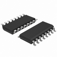
HEF4046BT,652 NXP Semiconductors, HEF4046BT,652 Datasheet - Page 5

HEF4046BT,652
Manufacturer Part Number
HEF4046BT,652
Description
IC PHASE-LOCK LOOP MCPWR 16SOIC
Manufacturer
NXP Semiconductors
Type
Phase Lock Loop (PLL)r
Series
HE4000Br
Specifications of HEF4046BT,652
Number Of Circuits
1
Package / Case
16-SOIC (3.9mm Width)
Pll
Yes
Input
Clock
Output
Clock
Ratio - Input:output
1:4
Differential - Input:output
No/No
Frequency - Max
2.7MHz
Divider/multiplier
No/No
Voltage - Supply
3 V ~ 15 V
Operating Temperature
-40°C ~ 85°C
Mounting Type
Surface Mount
Frequency-max
2.7MHz
Maximum Input Frequency
2.7 MHz
Minimum Input Frequency
1 MHz
Supply Voltage (max)
15 V
Supply Voltage (min)
3 V
Maximum Operating Temperature
+ 85 C
Minimum Operating Temperature
- 40 C
Input Level
CMOS
Mounting Style
SMD/SMT
Operating Supply Voltage
4.5 V to 15.5 V
Output Level
CMOS
Lead Free Status / RoHS Status
Lead free / RoHS Compliant
Lead Free Status / RoHS Status
Lead free / RoHS Compliant, Lead free / RoHS Compliant
Other names
568-3105-5
933372900652
HEF4046BTD
933372900652
HEF4046BTD
Philips Semiconductors
Phase comparator 2 is an edge-controlled digital memory
network. It consists of four flip-flops, control gating and a
3-state output circuit comprising p and n-type drivers
having a common output node. When the p-type or n-type
drivers are ON, they pull the output up to V
V
on the positive-going edges of the signals at SIGN
COMP
not of importance.
If the signal input frequency is higher than the comparator
input frequency, the p-type output driver is maintained ON
most of the time, and both the n and p-type drivers are
OFF (3-state) the remainder of the time. If the signal input
frequency is lower than the comparator input frequency,
the n-type output driver is maintained ON most of the time,
and both the n and p-type drivers are OFF the remainder
of the time. If the signal input and comparator input
frequencies are equal, but the signal input lags the
comparator input in phase, the n-type output driver is
maintained ON for a time corresponding to the phase
difference. If the comparator input lags the signal input in
phase, the p-type output driver is maintained ON for a time
corresponding to the phase difference. Subsequently, the
voltage at the capacitor of the low-pass filter connected to
this phase comparator is adjusted until the signal and
January 1995
SS
Phase-locked loop
respectively. This type of phase comparator only acts
IN
. Therefore, the duty factors of these signals are
Fig.5 Typical waveforms for phase-locked loop employing phase comparator 2 in locked condition.
DD
or down to
IN
and
5
comparator inputs are equal in both phase and frequency.
At this stable point, both p and n-type drivers remain OFF
and thus the phase comparator output becomes an open
circuit and keeps the voltage at the capacitor of the
low-pass filter constant.
Moreover, the signal at the phase comparator pulse output
(PCP
a locked condition. Thus, for phase comparator 2 no phase
difference exists between the signal and comparator
inputs over the full VCO frequency range. Moreover, the
power dissipation due to the low-pass filter is reduced
when this type of phase comparator is used because both
p and n-type output drivers are OFF for most of the signal
input cycle. It should be noted that the PLL lock range for
this type of phase comparator is equal to the capture
range, independent of the low-pass filter. With no signal
present at the signal input, the VCO is adjusted to its
lowest frequency for phase comparator 2 . Figure 5 shows
typical waveforms for a PLL employing this type of phase
comparator in locked condition.
OUT
) is a HIGH level which can be used for indicating
Product specification
HEF4046B
MSI


