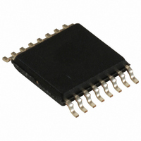
CY22150FZXC Cypress Semiconductor Corp, CY22150FZXC Datasheet - Page 6

CY22150FZXC
Manufacturer Part Number
CY22150FZXC
Description
IC CLOCK GEN PROG 16-TSSOP
Manufacturer
Cypress Semiconductor Corp
Type
Clock Generator, Fanout Distributionr
Datasheet
1.CY22150FZXC.pdf
(16 pages)
Specifications of CY22150FZXC
Number Of Circuits
1
Package / Case
16-TSSOP
Pll
Yes
Input
Crystal
Output
Clock
Ratio - Input:output
1:6
Differential - Input:output
No/No
Frequency - Max
200MHz
Divider/multiplier
Yes/No
Voltage - Supply
2.375 V ~ 3.465 V
Operating Temperature
0°C ~ 70°C
Mounting Type
Surface Mount
Frequency-max
200MHz
Maximum Input Frequency
133 MHz
Minimum Input Frequency
1 MHz
Output Frequency Range
80 KHz to 200 MHz
Supply Voltage (max)
7 V
Supply Voltage (min)
- 0.5 V
Maximum Operating Temperature
+ 70 C
Minimum Operating Temperature
0 C
Mounting Style
SMD/SMT
Operating Supply Voltage
3.3 V
Number Of Elements
1
Supply Current
45mA
Pll Input Freq (min)
1MHz
Pll Input Freq (max)
133MHz
Operating Supply Voltage (typ)
3.3V
Operating Temp Range
0C to 70C
Package Type
TSSOP
Operating Supply Voltage (min)
3.135V
Operating Supply Voltage (max)
3.465V
Operating Temperature Classification
Commercial
Pin Count
16
Lead Free Status / RoHS Status
Lead free / RoHS Compliant
For Use With
CY30700 - KIT PROG FOR CY22150428-1918 - KIT DEV FTG PROGRAMMING KIT428-1452 - SOCKET ADAPTER FOR CY22050
Lead Free Status / Rohs Status
Compliant
Other names
428-2176-5
CY22150FZXC
CY22150FZXC
Available stocks
Company
Part Number
Manufacturer
Quantity
Price
Company:
Part Number:
CY22150FZXC
Manufacturer:
CYPRESS
Quantity:
9
Part Number:
CY22150FZXC
Manufacturer:
CY
Quantity:
20 000
Stable operation of the CY22150 cannot be guaranteed if the
value of (P
100 MHz. Registers 40H, 41H, and 42H are defined in
PLL Post Divider Options [OCH(7..0)], [47H(7..0)]
The output of the VCO is routed through two independent
muxes, then to two divider banks to determine the final clock
output frequency. The mux determines if the clock signal feeding
into the divider banks is the calculated VCO frequency or REF.
There are two select muxes (DIV1SRC and DIV2SRC) and two
divider banks (Divider Bank 1 and Divider Bank 2) used to
determine this clock signal. The clock signal passing through
DIV1SRC and DIV2SRC is referred to as DIV1CLK and
DIV2CLK, respectively.
The divider banks have four unique divider options available: /2,
/3, /4, and /DIVxN. DIVxN is a variable that can be independently
programmed (DIV1N and DIV2N) for each of the two divider
banks. The minimum value of DIVxN is 4. The maximum value
Table 6. Input Load Capacitor Register Bit Settings
Table 7. P Counter Register Definition
Table 8. P Counter Register Definition
Table 9. PLL Post Divider Options
Table 10. Charge Pump Settings
Document #: 38-07104 Rev. *I
Address
Address
Address
Address
OCH
13H
40H
41H
42H
40H
41H
42H
47H
Charge Pump Setting – Pump(2..0)
total
CapLoad(7)
*(REF/Q
DIV1SRC
DIV2SRC
PB(7)
PB(7)
PO
PO
D7
D7
D7
D7
1
1
101, 110, 111
total
)) is above 400 MHz or below
000
001
010
100
011
CapLoad(6)
DIV1N(6)
DIV2N(6)
PB(6)
PB(6)
Q(6)
Q(6)
D6
D6
D6
D6
1
1
CapLoad(5)
DIV1N(5)
DIV2N(5)
PB(5)
PB(5)
Q(5)
Q(5)
D5
D5
D5
D5
0
0
Table
CapLoad(4)
DIV1N(4)
DIV2N(4)
Pump(2)
Pump(2)
8.
PB(4)
PB(4)
Q(4)
Q(4)
D4
D4
D4
D4
of DIVxN is 127. A value of DIVxN below 4 is not guaranteed to
work properly.
DIV1SRC is a single bit variable, controlled by register OCH. The
remaining seven bits of register OCH determine the value of post
divider DIV1N.
DIV2SRC is a single bit variable, controlled by register 47H. The
remaining seven bits of register 47H determine the value of post
divider DIV2N.
Register OCH and 47H are defined in
Charge Pump Settings [40H(2..0)]
The correct pump setting is important for PLL stability. Charge
pump settings are controlled by bits (4..2) of register 40H, and
are dependent on internal variable PB (see “PLL Frequency, P
Counter[40H(1..0)], [41H(7..0)], [42H(7)]”).
summarizes the proper charge pump settings, based on Ptotal.
See
Table 11
CapLoad(3)
DIV1N(3)
DIV2N(3)
Pump(1)
Pump(1)
PB(3)
PB(3)
Q(3)
Q(3)
D3
D3
Do not use – device will be unstable
D3
D3
on page 7 for register 40H bit locations and values.
Calculated P
CapLoad(2)
DIV1N(2)
DIV2N(2)
Pump(0)
Pump(0)
800 – 1023
PB(2)
480 – 639
640 – 799
PB(2)
Q(2)
45 – 479
Q(2)
16 – 44
D2
D2
D2
D2
total
CapLoad(1)
DIV1N(1)
DIV2N(1)
Table
PB(9)
PB(1)
PB(9)
PB(1)
Q(1)
Q(1)
D1
D1
D1
D1
Table 10
9.
CY22150
CapLoad(0)
Page 6 of 16
DIV1N(0)
DIV2N(0)
on page 6
PB(8)
PB(0)
PB(8)
PB(0)
Q(0)
Q(0)
D0
D0
D0
D0
[+] Feedback


