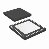
LMK02000ISQ/NOPB National Semiconductor, LMK02000ISQ/NOPB Datasheet

LMK02000ISQ/NOPB
Specifications of LMK02000ISQ/NOPB
LMK02000ISQTR
Available stocks
Related parts for LMK02000ISQ/NOPB
LMK02000ISQ/NOPB Summary of contents
Page 1
... The clock conditioner comes in a 48-pin LLP package and is footprint compatible with other clocking devices in the same family. Functional Block Diagram TRI-STATE ® registered trademark of National Semiconductor Corporation. © 2007 National Semiconductor Corporation Features ■ additive jitter ■ Integrated Integer-N PLL with outstanding normalized phase noise contribution of -224 dBc/Hz ■ ...
Page 2
Connection Diagram www.national.com 48-Pin LLP Package 2 20216502 ...
Page 3
Pin Descriptions Pin # 13, 16, 19, 22, 26, Vcc1, Vcc2, Vcc3, Vcc4, Vcc5, Vcc6, Vcc7, 30, 31, 33, 37, 40, 43, 46 Vcc8, Vcc9, Vcc10, Vcc11, Vcc12, Vcc13, Vcc14 ...
Page 4
... Absolute Maximum Ratings If Military/Aerospace specified devices are required, please contact the National Semiconductor Sales Office/ Distributors for availability and specifications. Parameter Power Supply Voltage Input Voltage Storage Temperature Range Lead Temperature (solder 4 s) Junction Temperature Recommended Operating Conditions Parameter Ambient Temperature Power Supply Voltage Note 1: " ...
Page 5
Symbol Parameter f Phase Detector Frequency COMP I CPout Charge Pump Source Current SRCE I CPout Charge Pump Sink Current SINK I TRI Charge Pump TRI-STATE CPout Magnitude of Charge Pump I %MIS CPout Sink vs. Source Current Mismatch Magnitude ...
Page 6
Symbol Parameter Clock Distribution Section (Note 9) - LVPECL Clock Outputs (CLKout3 to CLKout7) Jitter Additive RMS Jitter (Note 9) ADD t CLKoutX to CLKoutY (Note 10) SKEW V Output High Voltage OH V Output Low Voltage OL V Differential ...
Page 7
Note 12: Applies to CLKuWire, DATAuWire, and LEuWire. Serial Data Timing Diagram Data bits set on the DATAuWire signal are clocked into a shift register, MSB first, on each rising edge of the CLKuWire signal. On the rising edge of ...
Page 8
Charge Pump Current Specification Definitions I1 = Charge Pump Sink Current Charge Pump Sink Current Charge Pump Sink Current Charge Pump Source Current Charge ...
Page 9
Functional Description The LMK02000 precision clock conditioner combines the functions of jitter cleaning/reconditioning, multiplication, and distribution of a reference clock. The device integrates a high performance Integer-N Phase Locked Loop (PLL), three LVDS, and five LVPECL clock output distribution ...
Page 10
General Programming Information The LMK02000 device is programmed using several 32-bit registers which control the device's operation. The registers consist of a data field and an address field. The last 4 register bits, ADDR[3:0] form the address field. The ...
Page 11
CLKout0_EN CLKout1_EN CLKout2_EN CLKout3_EN CLKout4_EN CLKout5_EN CLKout6_EN CLKout7_EN RESET Register 11 www.national.com ...
Page 12
DIV4 PLL_CP_POL TRI-STATE POWERDOWN EN_CLKout_Global Register www.national.com 12 ...
Page 13
REGISTER Registers R0 through R7 control the eight clock outputs. Reg- ister R0 controls CLKout0, Register R1 controls CLKout1, and so on. There is one additional bit in register R0 called RESET. Aside from this, the ...
Page 14
CLKoutX_DIV[7:0] -- Clock Output Dividers These bits control the clock output divider value. In order for these dividers to be active, the respective CLKoutX_MUX (See 2.3.2) bit must be set to either "Divided" or "Divided and Delayed" mode. After ...
Page 15
PLL_MUX[3:0] -- Multiplexer Control for LD Pin These bits set the output mode of the LD pin. The table below lists several different modes. PLL_MUX[3:0] Output Type 0 Hi-Z 1 Push-Pull 2 Push-Pull 3 Push-Pull 4 Push-Pull 5 Push-Pull ...
Page 16
Application Information 3.1 SYSTEM LEVEL DIAGRAM The following shows the LMK02000 in a typical application. In this setup the clock may be multiplied, reconditioned, and redistributed. 3.2 BIAS PIN To properly use the device, bypass Bias (pin 36) with ...
Page 17
CURRENT CONSUMPTION / POWER DISSIPATION CALCULATIONS Due to the myriad of possible configurations the following ta- ble serves to provide enough information to allow the user to Block Condition Entire device, All outputs off; No LVPECL emitter resistors core ...
Page 18
To minimize junction temperature it is recommended that a simple heat sink be built into the PCB (if the ground plane layer is not exposed). This is done by including a copper area of about 2 square inches on the ...
Page 19
Physical Dimensions inches (millimeters) unless otherwise noted Order Number Package Marking LMK02000ISQ K02000 I LMK02000ISQX K02000 I Leadless Leadframe Package (Bottom View) 48 Pin LLP (SQA48A) Package Packing 250 Unit Tape and Reel 2500 Unit Tape and Reel 19 LVDS ...
Page 20
... National Semiconductor and the National Semiconductor logo are registered trademarks of National Semiconductor Corporation. All other brand or product names may be trademarks or registered trademarks of their respective holders. ...


