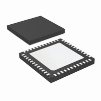
LMK02000ISQ/NOPB National Semiconductor, LMK02000ISQ/NOPB Datasheet - Page 4

LMK02000ISQ/NOPB
Manufacturer Part Number
LMK02000ISQ/NOPB
Description
IC CLOCK CONDITIONER PREC 48-LLP
Manufacturer
National Semiconductor
Type
Clock Conditionerr
Datasheet
1.LMK02000ISQNOPB.pdf
(20 pages)
Specifications of LMK02000ISQ/NOPB
Pll
Yes
Input
Clock
Output
LVDS, LVPECL
Number Of Circuits
1
Ratio - Input:output
2:8
Differential - Input:output
Yes/Yes
Frequency - Max
800MHz
Divider/multiplier
Yes/No
Voltage - Supply
3.15 V ~ 3.45 V
Operating Temperature
-40°C ~ 85°C
Mounting Type
Surface Mount
Package / Case
48-LLP
Frequency-max
800MHz
For Use With
LMK02000EVAL-1 - BOARD EVAL WITH 245.76 VCXOLMK02000EVAL2 - BOARD EVALUATION FOR LMK02000
Lead Free Status / RoHS Status
Lead free / RoHS Compliant
Other names
LMK02000ISQ
LMK02000ISQTR
LMK02000ISQTR
Available stocks
Company
Part Number
Manufacturer
Quantity
Price
Company:
Part Number:
LMK02000ISQ/NOPB
Manufacturer:
Intersil
Quantity:
106
www.national.com
I
I
f
V
f
SLEW
DUTY
P
CC
CC
OSCin
Fin
OSCin
Fin
Absolute Maximum Ratings
If Military/Aerospace specified devices are required, please contact the National Semiconductor Sales Office/ Distributors
for availability and specifications.
Recommended Operating Conditions
Note 1: "Absolute Maximum Ratings" indicate limits beyond which damage to the device may occur, including inoperability and degradation of device reliability
and/or performance. Functional operation of the device and/or non-degradation at the Absolute Maximum Ratings or other conditions beyond those indicated in
the Recommended Operating Conditions is not implied. The Recommended Operating Conditions indicate conditions at which the device is functional and the
device should not be operated beyond such conditions.
Note 2: This device is a high performance integrated circuit with ESD handling precautions. Handling of this device should only be done at ESD protected work
stations. The device is rated to a HBM-ESD of > 2 kV, a MM-ESD of > 200 V, and a CDM-ESD of > 1.2 kV.
Package Thermal Resistance
Note 3: Specification assumes 16 thermal vias connect the die attach pad to the embedded copper plane on the 4-layer JEDEC board. These vias play a key
role in improving the thermal performance of the LLP. It is recommended that the maximum number of vias be used in the board layout.
Electrical Characteristics
(3.15 V
parametric norms at Vcc = 3.3 V, T
and are not guaranteed).
Symbol
Power Supply Voltage
Input Voltage
Storage Temperature Range
Lead Temperature (solder 4 s)
Junction Temperature
Ambient Temperature
Power Supply Voltage
PD
square
Fin
square
Fin
≤
Vcc
Power Supply Current
(Note 5)
Power Down Current
Reference Oscillator Input Frequency
Range for Square Wave
Square Wave Input Voltage for OSCin and
OSCin*
Frequency Input Frequency Range
Frequency Input Slew Rate
Frequency Input Duty Cycle
Input Power Range for Fin or Fin*
Parameter
≤
3.45 V, -40 °C
Parameter
Parameter
48-Lead LLP (Note 3)
≤
T
A
A
= 25 °C, and at the Recommended Operation Conditions at the time of product characterization
Package
≤
85 °C, Differential Inputs/Outputs; except as specified. Typical values represent most likely
(Note 4)
Symbol
V
T
(Notes 1, 2)
CC
A
Current Consumption
Reference Oscillator
Symbol
Frequency Input
Entire device; CLKout0 & CLKout4
enabled in Bypass Mode
Entire device; All Outputs Off (no
emitter resistors placed)
POWERDOWN = 1
AC coupled; Differential (V
(Notes 6, 10)
AC coupled
T
V
V
T
T
STG
CC
IN
L
J
27.4° C/W
θ
4
JA
3.15
Min
-40
Conditions
θ
J-PAD (Thermal Pad)
-0.3 to (V
OD
5.8° C/W
Typ
3.3
25
-0.3 to 3.6
-65 to 150
)
Ratings
+260
125
CC
+ 0.3)
Min
-13
0.2
0.5
40
1
1
Max
3.45
85
145.8
Typ
70
1
Units
Max
200
800
1.6
°C
°C
°C
60
V
V
8
Units
°C
V
Units
MHz
MHz
dBm
V/ns
Vpp
mA
mA
%


