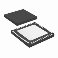
LMK02000ISQ/NOPB National Semiconductor, LMK02000ISQ/NOPB Datasheet - Page 15

LMK02000ISQ/NOPB
Manufacturer Part Number
LMK02000ISQ/NOPB
Description
IC CLOCK CONDITIONER PREC 48-LLP
Manufacturer
National Semiconductor
Type
Clock Conditionerr
Datasheet
1.LMK02000ISQNOPB.pdf
(20 pages)
Specifications of LMK02000ISQ/NOPB
Pll
Yes
Input
Clock
Output
LVDS, LVPECL
Number Of Circuits
1
Ratio - Input:output
2:8
Differential - Input:output
Yes/Yes
Frequency - Max
800MHz
Divider/multiplier
Yes/No
Voltage - Supply
3.15 V ~ 3.45 V
Operating Temperature
-40°C ~ 85°C
Mounting Type
Surface Mount
Package / Case
48-LLP
Frequency-max
800MHz
For Use With
LMK02000EVAL-1 - BOARD EVAL WITH 245.76 VCXOLMK02000EVAL2 - BOARD EVALUATION FOR LMK02000
Lead Free Status / RoHS Status
Lead free / RoHS Compliant
Other names
LMK02000ISQ
LMK02000ISQTR
LMK02000ISQTR
Available stocks
Company
Part Number
Manufacturer
Quantity
Price
Company:
Part Number:
LMK02000ISQ/NOPB
Manufacturer:
Intersil
Quantity:
106
EN_CLKout_Global
2.5.2 PLL_MUX[3:0] -- Multiplexer Control for LD Pin
These bits set the output mode of the LD pin. The table below
lists several different modes.
2.5.3 POWERDOWN Bit -- Device Power Down
This bit can power down the device. Enabling this bit powers
down the entire device and all blocks, regardless of the state
of any of the other bits or pins.
2.5.4 EN_CLKout_Global Bit -- Global Clock Output
Enable
This bit overrides the individual CLKoutX_EN bits (See 2.3.5).
When this bit is set to 0, all clock outputs are disabled, re-
gardless of the state of any of the other bits or pins. See 1.8
for more information on CLKout states.
PLL_MUX[3:0]
POWERDOWN bit
12 to 15
bit
10
11
0
1
0
1
2
3
4
5
6
7
8
9
0
1
Open Drain NMOS
Open Drain PMOS
Output Type
Push-Pull
Push-Pull
Push-Pull
Push-Pull
Push-Pull
Push-Pull
Push-Pull
Hi-Z
Entire Device Powered Down
Normal Operation (default)
Normal Operation (default)
Clock Outputs
Invalid
Invalid
Invalid
All Off
Digital Lock Detect
Digital Lock Detect
Mode
N Divider Output/2
R Divider Output/2
Disabled (default)
(50% Duty Cycle)
(50% Duty Cycle)
LD Pin Function
(Active High)
(Active Low)
Analog Lock
Analog Lock
Analog Lock
Logic High
Logic Low
Detect
Detect
Detect
15
2.5.5 PLL_CP_TRI Bit -- PLL Charge Pump TRI-STATE
This bit sets the PLL charge pump TRI-STATE.
2.5.6 PLL_CP_POLBbit -- PLL Charge Pump Polarity
This bit sets the polarity of the charge pump to either negative
or positive. A negative charge pump is used with a VCO or
VCXO which decreases frequency with increasing tuning volt-
age. A positive charge pump is used with a VCO or VCXO
which increases frequency with increasing tuning voltage.
2.6 Register R15
2.6.1 PLL_N[17:0] -- PLL N Divider
These bits program the divide value for the PLL N Divider.
The PLL N Divider precedes the PLL phase detector. The
VCO or VCXO frequency is calculated as, f
N Divider / PLL R Divider. Since the PLL N divider is a pure
binary counter, there are no illegal divide values for PLL_N
[17:0] except for 0.
2.6.2 PLL_CP_GAIN[1:0] -- PLL Charge Pump Gain
These bits set the charge pump gain of the PLL.
0 0 0 0 0 0 0 0 0 0 0 0 0 0 0 0 0 0
0 0 0 0 0 0 0 0 0 0 0 0 0 0 0 0 0 1
0 0 0 0 0 0 0 0 1 0 1 1 1 1 1 0 0 0
1 1 1 1 1 1 1 1 1 1 1 1 1 1 1 1 1 1
. . . . . . . . . . . . . . . . . .
. . . . . . . . . . . . . . . . . .
PLL_CP_TRI
PLL_CP_POL
PLL_CP_GAIN[1:0]
0
1
0
1
0
1
2
3
PLL_N[17:0]
PLL Charge Pump Polarity
Normal operation (default)
PLL Charge Pump
Negative (default)
Charge Pump Gain
TRI-STATE
1x (default)
Positive
VCO
16x
32x
4x
= f
www.national.com
OSCin
(default)
Divider
262143
PLL N
Invalid
Value
760
...
...
1
× PLL


