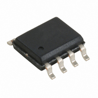
CY2304SXC-1 Cypress Semiconductor Corp, CY2304SXC-1 Datasheet - Page 4

CY2304SXC-1
Manufacturer Part Number
CY2304SXC-1
Description
IC CLK ZDB 4OUT 133MHZ 8SOIC
Manufacturer
Cypress Semiconductor Corp
Type
Fanout Distribution, Zero Delay Bufferr
Datasheet
1.CY2304SXC-2.pdf
(15 pages)
Specifications of CY2304SXC-1
Number Of Circuits
1
Package / Case
8-SOIC (3.9mm Width)
Pll
Yes
Input
Clock
Output
Clock
Ratio - Input:output
1:4
Differential - Input:output
No/No
Frequency - Max
133.3MHz
Divider/multiplier
No/No
Voltage - Supply
3 V ~ 3.6 V
Operating Temperature
0°C ~ 70°C
Mounting Type
Surface Mount
Frequency-max
133MHz
Output Frequency Range
10 MHz to 133.3 MHz
Supply Voltage (max)
3.6 V
Supply Voltage (min)
3 V
Maximum Operating Temperature
+ 70 C
Minimum Operating Temperature
0 C
Mounting Style
SMD/SMT
Operating Supply Voltage
3.3 V
Number Of Elements
1
Supply Current
45mA
Operating Supply Voltage (typ)
3.3V
Operating Temp Range
0C to 70C
Package Type
SOIC
Operating Supply Voltage (min)
3V
Operating Supply Voltage (max)
3.6V
Operating Temperature Classification
Commercial
Pin Count
8
Lead Free Status / RoHS Status
Lead free / RoHS Compliant
Lead Free Status / RoHS Status
Lead free / RoHS Compliant, Lead free / RoHS Compliant
Other names
428-2192-5
CY2304SXC-1
CY2304SXC-1
Available stocks
Company
Part Number
Manufacturer
Quantity
Price
Company:
Part Number:
CY2304SXC-1T
Manufacturer:
CY
Quantity:
158
Part Number:
CY2304SXC-1T
Manufacturer:
CYPRESS/赛普拉斯
Quantity:
20 000
CY2304
Zero Delay and Skew Control
Figure 2. REF. Input to CLKA/CLKB Delay vs. Difference in Loading Between FBK Pin and CLKA/CLKB Pins
To close the feedback loop of the CY2304, the FBK pin can be driven from any of the four available output pins. The output driving
the FBK pin is driving a total load of 7 pF, with any additional load that it drives. The relative loading of this output (with respect to the
remaining outputs) can adjust the input-output delay. This is shown in
Figure
2.
For applications requiring zero input-output delay, all outputs including the one providing feedback must be equally loaded. If
input-output delay adjustments are required, use the graph shown in
Figure 2
to calculate loading differences between the feedback
output and remaining outputs.
For zero output-output skew, be sure to load outputs equally. For further information on using CY2304, refer to the application note
AN1234
“CY2308: Zero Delay Buffer”.
Document Number: 38-07247 Rev. *J
Page 4 of 15
[+] Feedback


