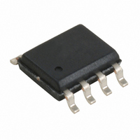
CY2304SXC-1 Cypress Semiconductor Corp, CY2304SXC-1 Datasheet - Page 5

CY2304SXC-1
Manufacturer Part Number
CY2304SXC-1
Description
IC CLK ZDB 4OUT 133MHZ 8SOIC
Manufacturer
Cypress Semiconductor Corp
Type
Fanout Distribution, Zero Delay Bufferr
Datasheet
1.CY2304SXC-2.pdf
(15 pages)
Specifications of CY2304SXC-1
Number Of Circuits
1
Package / Case
8-SOIC (3.9mm Width)
Pll
Yes
Input
Clock
Output
Clock
Ratio - Input:output
1:4
Differential - Input:output
No/No
Frequency - Max
133.3MHz
Divider/multiplier
No/No
Voltage - Supply
3 V ~ 3.6 V
Operating Temperature
0°C ~ 70°C
Mounting Type
Surface Mount
Frequency-max
133MHz
Output Frequency Range
10 MHz to 133.3 MHz
Supply Voltage (max)
3.6 V
Supply Voltage (min)
3 V
Maximum Operating Temperature
+ 70 C
Minimum Operating Temperature
0 C
Mounting Style
SMD/SMT
Operating Supply Voltage
3.3 V
Number Of Elements
1
Supply Current
45mA
Operating Supply Voltage (typ)
3.3V
Operating Temp Range
0C to 70C
Package Type
SOIC
Operating Supply Voltage (min)
3V
Operating Supply Voltage (max)
3.6V
Operating Temperature Classification
Commercial
Pin Count
8
Lead Free Status / RoHS Status
Lead free / RoHS Compliant
Lead Free Status / RoHS Status
Lead free / RoHS Compliant, Lead free / RoHS Compliant
Other names
428-2192-5
CY2304SXC-1
CY2304SXC-1
Available stocks
Company
Part Number
Manufacturer
Quantity
Price
Company:
Part Number:
CY2304SXC-1T
Manufacturer:
CY
Quantity:
158
Part Number:
CY2304SXC-1T
Manufacturer:
CYPRESS/赛普拉斯
Quantity:
20 000
Maximum Ratings
Supply voltage to ground potential.................–0.5 V to +7.0 V
DC input voltage (except Ref)...............–0.5 V to V
DC input voltage REF.............................................–0.5 V to 7 V
Operating Conditions for CY2304SXC Commercial Temperature Devices
Electrical Characteristics for CY2304SXC Commercial Temperature Devices
Document Number: 38-07247 Rev. *J
Notes
V
T
C
C
t
V
V
I
I
V
V
I
I
3. Applies to both REF clock and FBK.
4. Parameter is guaranteed by design and characterization. Not 100% tested in production.
PU
IL
IH
DD
DD
A
DD
IL
IH
OL
OH
L
IN
Parameter
Parameter
(PD mode) Power-down supply current REF = 0 MHz
Supply voltage
Operating temperature (ambient temperature)
Load capacitance (below 100 MHz)
Load capacitance (from 100 MHz to 133 MHz)
Input capacitance
Power-up time for all V
(power ramps must be monotonic)
Input LOW voltage
Input HIGH voltage
Input LOW current
Input HIGH current
Output LOW voltage
Output HIGH voltage
Supply current
Description
[3]
[4]
[4]
DD
s to reach minimum specified voltage
Description
V
V
I
I
Unloaded outputs, 100 MHz REF, Select
inputs at V
Unloaded outputs, 66 MHz REF (–1,–2)
Unloaded outputs, 33 MHz REF (–1,–2)
OL
OH
IN
IN
= 8 mA (–1, –2)
= 0 V
= V
= –8 mA (–1, –2)
DD
+ 0.5 V
DD
DD
Test Conditions
or GND
Storage temperature ..................................–65 °C to +150 °C
Junction temperature ..................................................150 °C
Static discharge voltage
(per MIL-STD-883, Method 3015).............................> 2000 V
0.05
Min
Min
3.0
2.0
2.4
0
–
–
–
–
–
–
–
–
–
–
–
100.0
Max
Max
50.0
45.0
12.0
32.0
18.0
3.6
0.8
0.4
70
30
15
50
7
–
–
CY2304
Page 5 of 15
Unit
Unit
ms
mA
mA
mA
°C
pF
pF
pF
A
A
A
V
V
V
V
V
[+] Feedback


