CY2308ZI-1H Cypress Semiconductor Corp, CY2308ZI-1H Datasheet - Page 3
CY2308ZI-1H
Manufacturer Part Number
CY2308ZI-1H
Description
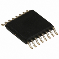
IC CLK ZDB 8OUT 133MHZ 16TSSOP
Manufacturer
Cypress Semiconductor Corp
Type
Fanout Distribution, Zero Delay Bufferr
Specifications of CY2308ZI-1H
Number Of Circuits
1
Package / Case
16-TSSOP
Pll
Yes with Bypass
Input
LVCMOS, LVTTL
Output
LVCMOS
Ratio - Input:output
1:8
Differential - Input:output
No/No
Frequency - Max
133.3MHz
Divider/multiplier
No/No
Voltage - Supply
3 V ~ 3.6 V
Operating Temperature
-40°C ~ 85°C
Mounting Type
Surface Mount
Frequency-max
133MHz
Output Frequency Range
10 MHz to 133.3 MHz
Supply Voltage (max)
3.6 V
Supply Voltage (min)
3 V
Maximum Operating Temperature
+ 85 C
Minimum Operating Temperature
- 40 C
Mounting Style
SMD/SMT
Operating Supply Voltage
3.3 V
Lead Free Status / RoHS Status
Contains lead / RoHS non-compliant
Other names
428-1355
Available stocks
Company
Part Number
Manufacturer
Quantity
Price

Part Number:
CY2308ZI-1H
Manufacturer:
CYPRESS/赛普拉斯
Quantity:
20 000
Company:
Part Number:
CY2308ZI-1HT
Manufacturer:
TI
Quantity:
560


Pinouts
Table 1. Pin Definitions - 16 Pin SOIC
Select Input Decoding
Document Number: 38-07146 Rev. *L
Notes
1. Weak pull down.
2. Weak pull down on all outputs.
3. Weak pull ups on these inputs.
4. Outputs inverted and PLL bypass mode for 2308–2 and 2308–3, S2 = 1 and S1 = 0.
Pin
S2
10
12
13
14
15
16
11
1
2
3
4
5
6
7
8
9
0
0
1
1
REF
CLKA1
CLKA2
V
GND
CLKB1
CLKB2
S2
S1
CLKB3
CLKB4
GND
V
CLKA3
CLKA4
FBK
DD
DD
[3]
[3]
[1]
S1
0
1
0
1
[2]
[2]
[2]
[2]
[2]
[2]
[2]
[2]
Signal
CLOCK A1–A4
Driven
Tri-state
Driven
Driven
Figure 1. Pin Diagram - 16 Pin SOIC (Top view)
Power supply ground
Input reference frequency
Clock output, Bank A
Clock output, Bank A
Power supply voltage
Power supply ground
Clock output, Bank B
Clock output, Bank B
Select input, bit 2
Select input, bit 1
Clock output, Bank B
Clock output, Bank B
Power supply voltage
Clock output, Bank A
Clock output, Bank A
PLL feedback input
[4]
CLKA1
CLKA2
CLKB1
CLKB2
GND
REF
V
S2
DD
CLOCK B1–B4
1
2
3
4
5
6
7
8
Driven
Tri-state
Tri-state
Driven
[4]
15
14
13
12
11
10
16
9
FBK
CLKA4
CLKA3
V
GND
CLKB4
CLKB3
S1
DD
Description
Output Source
Reference
PLL
PLL
PLL
PLL Shutdown
Y
N
Y
N
CY2308
Page 3 of 17
[+] Feedback
Related parts for CY2308ZI-1H
Image
Part Number
Description
Manufacturer
Datasheet
Request
R

Part Number:
Description:
Manufacturer:
Cypress Semiconductor Corp
Datasheet:
Part Number:
Description:
Manufacturer:
Cypress Semiconductor Corp
Datasheet:
Part Number:
Description:
Manufacturer:
Cypress Semiconductor Corp
Datasheet:
Part Number:
Description:
Manufacturer:
Cypress Semiconductor Corp
Datasheet:
Part Number:
Description:
Manufacturer:
Cypress Semiconductor Corp
Datasheet: