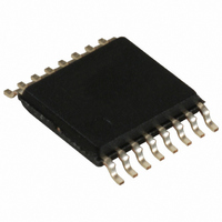
CY2308ZI-1H Cypress Semiconductor Corp, CY2308ZI-1H Datasheet - Page 4

CY2308ZI-1H
Manufacturer Part Number
CY2308ZI-1H
Description
IC CLK ZDB 8OUT 133MHZ 16TSSOP
Manufacturer
Cypress Semiconductor Corp
Type
Fanout Distribution, Zero Delay Bufferr
Specifications of CY2308ZI-1H
Number Of Circuits
1
Package / Case
16-TSSOP
Pll
Yes with Bypass
Input
LVCMOS, LVTTL
Output
LVCMOS
Ratio - Input:output
1:8
Differential - Input:output
No/No
Frequency - Max
133.3MHz
Divider/multiplier
No/No
Voltage - Supply
3 V ~ 3.6 V
Operating Temperature
-40°C ~ 85°C
Mounting Type
Surface Mount
Frequency-max
133MHz
Output Frequency Range
10 MHz to 133.3 MHz
Supply Voltage (max)
3.6 V
Supply Voltage (min)
3 V
Maximum Operating Temperature
+ 85 C
Minimum Operating Temperature
- 40 C
Mounting Style
SMD/SMT
Operating Supply Voltage
3.3 V
Lead Free Status / RoHS Status
Contains lead / RoHS non-compliant
Other names
428-1355
Available stocks
Company
Part Number
Manufacturer
Quantity
Price
Part Number:
CY2308ZI-1H
Manufacturer:
CYPRESS/赛普拉斯
Quantity:
20 000
Company:
Part Number:
CY2308ZI-1HT
Manufacturer:
TI
Quantity:
560
Available CY2308 Configurations
Zero Delay and Skew Control
To close the feedback loop of the CY2308, the user has to
connect any one of the eight available output pins to FBK pin.
The output driving the FBK pin drives a total load of 7 pF plus
any additional load that it drives. The relative loading of this
output to the remaining outputs adjusts the input-output delay as
shown in the
For applications requiring zero input-output delay, all outputs
including the one providing feedback is equally loaded.
Document Number: 38-07146 Rev. *L
Notes
CY2308–1
CY2308–1H
CY2308–2
CY2308–2
CY2308–3
CY2308–3
CY2308–4
CY2308–5H
5. User has to select one of the available outputs that drive the feedback pin and need to connect selected output pin to FBK pin externally.
6. Output phase is indeterminant (0° or 180° from input clock). If phase integrity is required, use CY2308–2.
Figure 2. REF. Input to CLKA/CLKB Delay Versus Difference in Loading Between FBK Pin and CLKA/CLKB Pins
Device
Figure
2.
Bank A or Bank B
Bank A or Bank B
Bank A
Bank B
Bank A
Bank B
Bank A or Bank B
Bank A or Bank B
Feedback From
[5]
Reference
Reference
Reference
2 x Reference
2 x Reference
4 x Reference
2 x Reference
Reference /2
Bank A Frequency
If input-output delay adjustments are required, use the
Delay and Skew Control
between the feedback output and remaining outputs.
For zero output-output skew, outputs are loaded equally. For
further information on using CY2308, refer to the application note
CY2308: Zero Delay
Reference
Reference
Reference/2
Reference
Reference
2 x Reference
2 x Reference
Reference /2
Buffer-AN1234.
graph to calculate loading differences
[6]
Bank B Frequency
CY2308
Page 4 of 17
Zero
[+] Feedback


