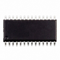
TDA7427AD1 STMicroelectronics, TDA7427AD1 Datasheet - Page 8

TDA7427AD1
Manufacturer Part Number
TDA7427AD1
Description
IC SYNTHESIZER/IF COUNTER SO-28
Manufacturer
STMicroelectronics
Type
PLL Frequency Synthesizerr
Datasheet
1.TDA7427AD1.pdf
(21 pages)
Specifications of TDA7427AD1
Pll
Yes
Input
Clock, Crystal
Output
Clock, Crystal
Number Of Circuits
1
Ratio - Input:output
3:1
Differential - Input:output
No/No
Frequency - Max
290MHz
Divider/multiplier
Yes/No
Voltage - Supply
4.5 V ~ 11 V
Operating Temperature
-40°C ~ 85°C
Mounting Type
Surface Mount
Package / Case
28-SOIC (7.5mm Width)
Frequency-max
290MHz
Lead Free Status / RoHS Status
Lead free / RoHS Compliant
Available stocks
Company
Part Number
Manufacturer
Quantity
Price
Part Number:
TDA7427AD1
Manufacturer:
ST
Quantity:
20 000
TDA7427A
Figure 2. AM direct mode operation for SW, MW and LW
DIVIDER FROM VCO FREQUENCY TO
REFERENCE FREQUENCY
This divider provides a low frequency f
phase is compared with the reference frequency
f
and PC5 to PC15
OPERATING MODES
Four operating modes are available fo PLL; they
are user programmable with the Mode PM regis-
ters (see table below).
8/21
REF
- Standby mode: in this mode all device func-
- FM and AM (SW) Swallow Mode (SW):
PM0
. It is controlled by the registers PC0 to PC4
tions are stopped. This allows low current
consumption without loss of information in all
registers. The pin LP-OUT is forced to 0V,
and all data registers are set to EFH. The os-
cillator keeps running.
in this mode the FM or AM signal is applied to
a 32/33 prescaler, which is controlled by a 5
bit divider ’A’.The 5 bit register (PC0 to PC4)
controls this divider. In parallel the output of
the prescaler is connected to a 11 bit divider
’B’. (PC5 to PC15).
f
0
1
0
1
OSC
= (R+1) f
PM1
OSC IN
0
0
1
1
AM IN
FM IN
REF
Operating Mode
AM (swallow)
AM (direct)
Standby
FM
SYN
PREDIVIDER
PRESCALER
RC0 ... RC15
PC0 ... PC15
REGISTER
REGISTER
which
: R
: C
THREE STATE PHASE COMPARATOR
The phase comparator generates a phase error
signal according to phase difference between
f
charge pump current generator (fig. 3)
CHARGE PUMP CURRENT GENERATOR
This stage generates signed pulses of current.
The phase error signal decides the duration and
polarity of those pulses.
The current absolute values are programmable by
A0, A1, A2 registers for high current and B0, B1,
registers for low current.
LOW NOISE CMOS OP-AMP
An internal voltage divider at pin VREF connects
the positive input of the low noise Op-Amp. The
charge pump output connects the negative input.
This internal amplifier in cooperation with external
components can provide an active filter.
SYN
- AM direct mode: the AM signal is applied di-
Dividing range:
f
Dividing range calculation :
f
f
Important:for correct operationA 32, B A,with
A andB variable values of the dividers).
rectly to the 16 bit static divider ’C’. (PC0 to
PC15)
f
VCO
VCO
VCO
OSC
fsyn
and f
fref
D95AU376A
= (C + 1) f
= [ 33 A + (B + 1 - A) 32 ] f
= (32 B + A + 32) f
= (R + 1) f
REF
DETECTOR
PHASE
. This phase error signal drives the
REF
REF
TO CHARGE
PUMP
REF
REF


