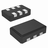
CY2XF24FLXIT Cypress Semiconductor Corp, CY2XF24FLXIT Datasheet - Page 7

CY2XF24FLXIT
Manufacturer Part Number
CY2XF24FLXIT
Description
IC XTAL OSC LVPECL I2C 6CLCC
Manufacturer
Cypress Semiconductor Corp
Datasheet
1.CY2XF24FLXCT.pdf
(15 pages)
Specifications of CY2XF24FLXIT
Pll
Yes
Input
Crystal
Output
LVPECL
Number Of Circuits
1
Ratio - Input:output
1:1
Differential - Input:output
No/Yes
Frequency - Max
690MHz
Divider/multiplier
Yes/No
Voltage - Supply
*
Operating Temperature
*
Mounting Type
Surface Mount
Package / Case
6-CLCC
Frequency
*
Count
*
Operating Supply Voltage (typ)
2.5/3.3
Output Level
LVPECL
Symmetry Max
60%
Operating Temp Range
-40C to 85C
Screening Level
Industrial
Lead Free Status / RoHS Status
Lead free / RoHS Compliant
Absolute Maximum Conditions
Operating Conditions
DC Electrical Characteristics
Document Number: 001-53146 Rev. *D
V
V
T
T
ESD
Θ
V
T
T
I
V
V
V
V
V
Notes
Parameter
Parameter
Parameter
DD
2. The voltage on any input or IO pin cannot exceed the power pin during power up.
3. Simulated. The board is derived from the JEDEC multilayer standard. It measures 76 x 114 x 1.6 mm and has 4-layers of copper (2/1/1/2 oz.). The internal layers
4. I
A
DD
IN
S
J
DD
PU
OH
OL
OD1
OD2
OCM
JA
[2]
[4]
[3]
are 100% copper planes, while the top and bottom layers have 50% metalization. No vias are included in the model.
DD
HBM
SDA
includes ~24 mA of current that is dissipated externally in the output termination resistors.
SCLK
START
3.3-V supply voltage range
2.5-V supply voltage range
Power-up time for V
monotonic)
Ambient temperature (commercial)
Ambient temperature (industrial)
Operating supply current
LVPECL high output voltage
LVPECL low output voltage
LVPECL output voltage swing
(V
LVPECL output voltage swing
(V
LVPECL output common mode
voltage (V
Supply voltage
Input voltage, DC
Temperature, storage
Temperature, junction
Electrostatic discharge (ESD) protection
human body model (HBM)
Thermal resistance, junction to ambient
OH
OH
- V
- V
DA6
OL
OL
Figure 7. Frame Format (Device Address, R/W, Register Address, Register Data)
OH
)
)
Description
DA5 DA0
+ V
Description
+
+
OL
)/2
DD
to reach minimum specified voltage (power ramp is
R/W
ACK
Description
PRELIMINARY
V
terminated
V
terminated
V
V
V
V
V
V
V
1.5 V
V
1.5 V
DD
DD
DD
DD
DD
DD
DD
DD
DD
DD
RA7
= 3.465 V, CLK = 150 MHz, output
= 2.625 V, CLK = 150 MHz, output
= 3.3 V or 2.5 V, R
– 2.0 V
= 3.3 V or 2.5 V, R
– 2.0 V
= 3.3 V or 2.5 V, R
– 2.0 V
= 2.5 V, R
= 2.5 V, R
Relative to V
Non Operating
JEDEC STD 22-A114-B
0 m/s airflow
RA6 RA1
+
+
Condition
TERM
TERM
Condition
= 50 Ω to V
= 50 Ω to V
SS
RA0
TERM
TERM
TERM
= 50 Ω to
= 50 Ω to
= 50 Ω to
ACK
DD
DD
–
–
D7
V
V
DD
DD
3.135
2.375
D6
0.05
Min
Min
600
500
–40
1.2
2000
–0.5
–0.5
– 1.15
Min
0
–
–
–55
–40
– 2.0
+
+
D1
Typ
Typ
64
3.3
2.5
–
–
–
–
–
–
–
–
–
–
D0
V
DD
Max
135
135
4.4
–
V
V
ACK
1.625
3.465
2.625
+0.5
1000
1000
Max
0.75
Max
150
145
500
DD
DD
70
85
–
CY2XF24
–
–
Page 7 of 15
°C/W
Unit
Unit
Unit
mA
mA
mV
mV
STOP
ms
°C
°C
°C
°C
V
V
V
V
V
V
V
V
[+] Feedback


