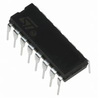
HCF4536BEY STMicroelectronics, HCF4536BEY Datasheet

HCF4536BEY
Specifications of HCF4536BEY
Available stocks
Related parts for HCF4536BEY
HCF4536BEY Summary of contents
Page 1
... Selection outputs is accomplished by the decoder and the BCD inputs and D. MONO IN is the timing input HCF4536B DIP TUBE T & R HCF4536BEY can be achieved using 1/13 ...
Page 2
Grounding of the MONO IN terminal through a resistor higher, disables the one shot circuit and connects the decoder directly to the DECODE OUT terminal. A resistor ground ...
Page 3
TRUTH TABLE In1 Set Reset Don’t Care DECODE OUT SELECTION TABLE ...
Page 4
HCF4536B LOGIC DIAGRAM 4/13 ...
Page 5
LOGIC DIAGRAM ABSOLUTE MAXIMUM RATINGS Symbol V Supply Voltage Input Voltage Input Current I Power Dissipation per Package P D Power Dissipation per Output Transistor T Operating Temperature op T Storage Temperature stg Absolute ...
Page 6
HCF4536B RECOMMENDED OPERATING CONDITIONS Symbol V Supply Voltage DD V Input Voltage I T Operating Temperature op DC SPECIFICATIONS Symbol Parameter V (V) I Quiescent Current 0/5 L 0/10 0/15 0/20 V High Level Output 0/5 OH Voltage 0/10 0/15 ...
Page 7
DYNAMIC ELECTRICAL CHARACTERISTICS (T Symbol Parameter t t Propagation Delay Time PLH PHL (Clock to Q1, 8-Bypass High) Propagation Delay Time (Clock to Q1, 8-Bypass Low) Propagation Delay Time (Clock to Q16) Propagation Delay Time (Qn to Qn+1) t Propagation ...
Page 8
HCF4536B TYPICAL APPLICATIONS Time Internal Configuration Using External Clock; Set and Clock Inhibit Functions Time Internal Configuration Using Ext. Ck; Reset and Output Monostable to Achieve a Pulse Out TIMING DIAGRAM 8/13 Time Internal Configuration Using On-Chip RC oscillator and ...
Page 9
Inputs In 1 Set Reset FUNCTIONAL TEST SEQUENCE Test function has been included for the reduction of test time required to exercise all ...
Page 10
HCF4536B WAVEFORM : PROPAGATION DELAY TIMES, PULSE WIDTH CLOCK 10/13 ...
Page 11
Plastic DIP-16 (0.25) MECHANICAL DATA mm. DIM. MIN. TYP a1 0.51 B 0.77 b 0 8.5 e 2.54 e3 17. 3.3 Z inch MAX. MIN. TYP. 0.020 1.65 0.030 0.020 0.010 20 0.335 ...
Page 12
SO-16 MECHANICAL DATA mm. DIM. MIN. TYP 0.35 b1 0. 9.8 E 5.8 e 1.27 e3 8.89 F 3.8 G 4 inch MAX. MIN. TYP. 1.75 0.2 ...
Page 13
... No license is granted by implication or otherwise under any patent or patent rights of STMicroelectronics. Specifications mentioned in this publication are subject to change without notice. This publication supersedes and replaces all information previously supplied ...


