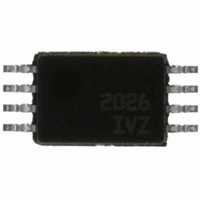
ISL12026IVZ-T Intersil, ISL12026IVZ-T Datasheet - Page 16

ISL12026IVZ-T
Manufacturer Part Number
ISL12026IVZ-T
Description
IC RTC/CALENDAR EEPROM 8-TSSOP
Manufacturer
Intersil
Type
Clock/Calendar/EEPROMr
Datasheet
1.ISL12026IBZ-T.pdf
(24 pages)
Specifications of ISL12026IVZ-T
Memory Size
4K (512 x 8)
Time Format
HH:MM:SS (12/24 hr)
Date Format
YY-MM-DD-dd
Interface
I²C, 2-Wire Serial
Voltage - Supply
2.7 V ~ 5.5 V
Operating Temperature
-40°C ~ 85°C
Mounting Type
Surface Mount
Package / Case
8-TSSOP
Rohs Compliant
YES
Lead Free Status / RoHS Status
Lead free / RoHS Compliant
Other names
ISL12026IVZ-TTR
Available stocks
Company
Part Number
Manufacturer
Quantity
Price
Following the Slave Byte is a two byte word address. The
word address is either supplied by the master device or
obtained from an internal counter. On power up the internal
address counter is set to address 0h, so a current address
read of the EEPROM array starts at address 0. When
required, as part of a random read, the master must supply
the 2 Word Address Bytes as shown in Figure 15.
In a random read operation, the slave byte in the “dummy
write” portion must match the slave byte in the “read”
section. That is if the random read is from the array the slave
byte must be 1010111x in both instances. Similarly, for a
random read of the Clock/Control Registers, the slave byte
must be 1101111x in both places.
Write Operations
Byte Write
For a write operation, the device requires the Slave Address
Byte and the Word Address Bytes. This gives the master
access to any one of the words in the array or CCR. (Note:
Prior to writing to the CCR, the master must write a 02h, then
06h to the status register in two preceding operations to
enable the write operation. See “Writing to the Clock/Control
Registers” on page 12). Upon receipt of each address byte,
the ISL12026 responds with an acknowledge. After receiving
ARRAY
CCR
SIGNALS FROM
THE MASTER
SDA BUS
SIGNALS FROM
THE SLAVE
A7
1
1
D7
FIGURE 15. SLAVE ADDRESS, WORD ADDRESS, AND DATA BYTES (16 BYTE PAGES)
0
DEVICE IDENTIFIER
16
A6
0
1
D6
0
A5
D5
1
0
0
S
T
A
R
T
1
ADDRESS
A4
SLAVE
D4
FIGURE 16. BYTE WRITE SEQUENCE
0
1
0
ISL12026, ISL12026A
1
1
1
A3
D3
1
0
0
A
C
K
0 0 0 0 0 0 0
ADDRESS 1
WORD
A2
D2
1
0
both address bytes the ISL12026 awaits the 8 bits of data.
After receiving the 8 data bits, the ISL12026 again responds
with an acknowledge. The master then terminates the
transfer by generating a stop condition. The ISL12026 then
begins an internal write cycle of the data to the non-volatile
memory. During the internal write cycle, the device inputs
are disabled, so the device will not respond to any requests
from the master. The SDA output is at high impedance (see
Figure 16).
A write to a protected block of memory is ignored, but will still
receive an acknowledge. At the end of the write command,
the ISL12026 will not initiate an internal write cycle, and will
continue to ACK commands.
Byte writes to all of the non-volatile registers are allowed,
except the DWAn registers which require multiple byte writes
or page writes to trigger non-volatile writes. See “Device
Operation” on page 12 for more information.
Page Write
The ISL12026 has a page write operation. It is initiated in the
same manner as the byte write operation; but instead of
terminating the write cycle after the first data byte is
transferred, the master can transmit up to 15 more bytes to
the memory array and up to 7 more bytes to the clock/control
registers. The RTC registers require a page write (8 bytes),
A1
D1
1
0
A
C
K
ADDRESS 0
WORD
R/W
A8
A0
D0
A
C
K
SLAVE ADDRESS BYTE
WORD ADDRESS 1
WORD ADDRESS 0
DATA
DATA BYTE
BYTE 0
BYTE 3
BYTE 1
BYTE 2
A
C
K
O
S
T
P
November 30, 2010
FN8231.9


