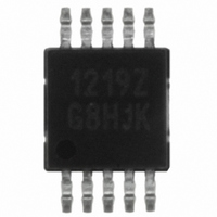
ISL1219IUZ Intersil, ISL1219IUZ Datasheet - Page 15

ISL1219IUZ
Manufacturer Part Number
ISL1219IUZ
Description
IC RTC LP BATT BACK SRAM 10MSOP
Manufacturer
Intersil
Type
Clock/Calendar/NVSRAMr
Specifications of ISL1219IUZ
Memory Size
2B
Time Format
HH:MM:SS (12/24 hr)
Date Format
YY-MM-DD-dd
Interface
I²C, 2-Wire Serial
Voltage - Supply
2.7 V ~ 5.5 V
Operating Temperature
-40°C ~ 85°C
Mounting Type
Surface Mount
Package / Case
10-MSOP, Micro10™, 10-uMAX, 10-uSOP
Clock Format
HH
Clock Ic Type
RTC
Interface Type
I2C, Serial
Memory Configuration
2 X 8
Supply Voltage Range
2.7V To 5.5V
Digital Ic Case Style
MSOP
Rohs Compliant
Yes
Lead Free Status / RoHS Status
Lead free / RoHS Compliant
Available stocks
Company
Part Number
Manufacturer
Quantity
Price
Company:
Part Number:
ISL1219IUZ
Manufacturer:
Intersil
Quantity:
490
Company:
Part Number:
ISL1219IUZ
Manufacturer:
Intersil
Quantity:
222
Part Number:
ISL1219IUZ-T
Manufacturer:
INTERSIL
Quantity:
20 000
EVENT DETECTION REGISTER (EV)
The ISL1219 provides an easy to use event and tamper
detection circuit. The Event Detection Register configures
the functionality of the event detection circuits.
EVENT INPUT SAMPLING SELECTION BITS
(ESMP<1:0>)
These two bits select the rate of sampling of the EVIN pin to
trigger an event detection. For example, a 2Hz sampling rate
would configure the ISL1219 to check the status of the EV
pin twice a second. Slower sampling significantly reduces
the supply current drain.
EVENT INPUT TIME BASE HYSTERESIS SELECTION
BITS (EHYS<1:0>)
These two bits select the time base hysteresis of the EVIN
pin to filter bouncing or noise of external event detection
circuits. The time filter can be set between 0 to 31.25 ms.
EVENT DETECT ENABLE BIT (EVEN)
This bit enables/disables the Event Detect function of the
ISL1219. When this bit is set to “1”, the Event Detect and
Time Stamp are active. When this bit is cleared to “0”, the
Event Detect and Time Stamp are disabled. Only the first
Event is Time Stamped in a series of Events between Event
resets (see EVT bit in the Status Register).
RTC HALT ON EVENT DETECT BIT (RTCHLT)
This bit sets the RTC registers to continue or halt counting
upon an Event Detect triggered by the EV pin. The time
keeping function will cease when RTCHLT is set to “1”, the
RTC will discontinue incrementing if an event is detected.
Counting will resume when there is a valid write to the to the
RTC registers (i.e. time set). The RTCHLT is cleared to “0”
after the write to the RTC registers.
Note: This function requires that the event detection is
enabled (see EVEN bit).
ESMP1
EHYS1
0
0
1
1
0
0
1
1
ESMP0
EHYS0
0
1
0
1
0
1
0
1
TABLE 10.
TABLE 11.
15
TIME BASE HYSTERESIS
EVENT SAMPLING RATE
0 (pull-up always on)
Always ON
15.625ms
31.25ms
3.9ms
1
2Hz
1Hz
/
4
Hz
ISL1219
EVENT OUTPUT IN BATTERY MODE ENABLE BIT
(EVBATB)
This bit enables/disables the EVDET pin during battery
backup mode (i.e. V
is set to “1”, the Event Detect Output is disabled in battery
backup mode. When the EVBATB is cleared to “0”, the Event
Detect output is enabled in battery backup mode.This
feature can be used to save power during battery mode.
EVENT CURRENT SOURCE ENABLE BIT (EVIENB)
This bit enables/disables the internal pull-up current source
used for the EVIN pin. When the EVIENB bit is set to “1”, the
pull-up current source is always disabled. When the EVIENB
bit is cleared to “0”, the pull-up current source is enabled
(current source is approximately 1µA).
Analog Trimming Register
ANALOG TRIMMING REGISTER (ATR<5:0>)
Six analog trimming bits, ATR0 to ATR5, are provided in
order to adjust the on-chip load capacitance value for
frequency compensation of the RTC. Each bit has a different
weight for capacitance adjustment. For example, using a
Citizen CFS-206 crystal with different ATR bit combinations
provides an estimated ppm adjustment range from -34 to
+80ppm to the nominal frequency compensation. The
combination of analog and digital trimming can give up to -94
to +140ppm of total adjustment.
The effective on-chip series load capacitance, C
ranges from 4.5pF to 20.25pF with a mid-scale value of
12.5pF (default). C
controlled capacitors, C
and X2 pins to ground (see Figure 11). The value of C
C
The effective series load capacitance is the combination of
C
C
C
C X
X2
X1
LOAD
LOAD
=
is given by the following formula:
and C
(
16 b5
=
=
⋅
---------------------------------- -
⎛
⎝
⎛
⎝
16 b5
---------------------------------------------------------------------------------------------------------------------------- -
X2
---------- -
C
1
X1
+
⋅
:
8 b4
X1
X2
1
+
FIGURE 13. DIAGRAM OF ATR
⋅
---------- -
C
+
1
8 b4
X2
LOAD
+
⋅
BAT
4 b3
⎞
⎠
C
C
X1
X2
⋅
+
X1
pin supply ON). When the EVBATB
4 b3
is changed via two digitally
+
⋅
and C
2 b2
⋅
+
2 b2
2
+
⋅
X2
1 b1
OSCILLATOR
⋅
, connected from the X1
+
CRYSTAL
1 b1
+
⋅
0.5 b0
+
⋅
0.5 b0
+
⋅
9
LOAD
)pF
August 14, 2006
+
9
⎞ pF
⎠
X1
,
FN6314.1
and


