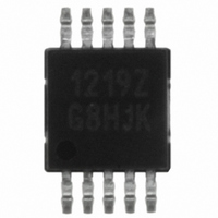
ISL1219IUZ Intersil, ISL1219IUZ Datasheet - Page 8

ISL1219IUZ
Manufacturer Part Number
ISL1219IUZ
Description
IC RTC LP BATT BACK SRAM 10MSOP
Manufacturer
Intersil
Type
Clock/Calendar/NVSRAMr
Specifications of ISL1219IUZ
Memory Size
2B
Time Format
HH:MM:SS (12/24 hr)
Date Format
YY-MM-DD-dd
Interface
I²C, 2-Wire Serial
Voltage - Supply
2.7 V ~ 5.5 V
Operating Temperature
-40°C ~ 85°C
Mounting Type
Surface Mount
Package / Case
10-MSOP, Micro10™, 10-uMAX, 10-uSOP
Clock Format
HH
Clock Ic Type
RTC
Interface Type
I2C, Serial
Memory Configuration
2 X 8
Supply Voltage Range
2.7V To 5.5V
Digital Ic Case Style
MSOP
Rohs Compliant
Yes
Lead Free Status / RoHS Status
Lead free / RoHS Compliant
Available stocks
Company
Part Number
Manufacturer
Quantity
Price
Company:
Part Number:
ISL1219IUZ
Manufacturer:
Intersil
Quantity:
490
Company:
Part Number:
ISL1219IUZ
Manufacturer:
Intersil
Quantity:
222
Part Number:
ISL1219IUZ-T
Manufacturer:
INTERSIL
Quantity:
20 000
V
This input provides a backup supply voltage to the device.
V
supply fails. This pin can be connected to a battery, a Super
Cap or tied to ground if not used.
EVIN (Event Input)
The EVIN pin is an input that is used to detect an externally
monitored event. When a high signal is present at the EVIN
pin, an “event” is detected. This input may be used for
various monitoring functions, such as the opening of a
detection switch on a chassis or door. The event detection
circuit can be user enabled or disabled (see EVEN bit) and
provides the option to be operational in battery backup
modes (see EVBATB bit). When the event detection is
disabled the EVIN pin is gated OFF. See “Functional
Description” on page 8 for more details.
EVDET (Event Detect Output)
The EVDET is an open drain output which will go low when
an event is detected at the EVIN pin. If the event detection
function is enabled, the EVDET output will go low and stay
low until the EVT bit is cleared (see EVIN pin description).
IRQ/F
This dual function pin can be used as an interrupt or
frequency output pin. The IRQ/F
the frequency out control bits of the control/status register.
• Interrupt Mode. The pin provides an interrupt signal
• Frequency Output Mode. The pin outputs a clock signal
Serial Clock (SCL)
The SCL input is used to clock all serial data into and out of
the device. The input buffer on this pin is always active (not
gated). It is disabled when the backup power supply on the
V
Serial Data (SDA)
SDA is a bidirectional pin used to transfer data into and out
of the device. It has an open drain output and may be ORed
with other open drain or open collector outputs. The input
buffer is always active (not gated) in normal mode.
An open drain output requires the use of a pull-up resistor.
The output circuitry controls the fall time of the output signal
with the use of a slope controlled pull-down. The circuit is
designed for 400kHz I
when the backup power supply on the V
BAT
BAT
BAT
output. This signal notifies a host processor that an alarm
has occurred and requests action. It is an open drain
active low output.
which is related to the crystal frequency. The frequency
output is user selectable and enabled via the I
an open drain active low output.
supplies power to the device in the event that the V
pin is activated to minimize power consumption.
OUT
(Interrupt Output/Frequency Output)
2
C interface speeds. It is disabled
8
OUT
mode is selected via
BAT
pin is activated.
2
C bus. It is
DD
ISL1219
V
Chip power supply and ground pins. The device will operate
with a power supply from V
capacitor is recommended on the V
Functional Description
Power Control Operation
The power control circuit accepts a V
Many types of batteries can be used with Intersil RTC
products. For example, 3.0V or 3.6V Lithium batteries are
appropriate, and battery sizes are available that can power
the ISL1219 for up to 10 years. Another option is to use a
Super Cap for applications where V
to a month. See the “Application Section” on page 20 for
more information.
Normal Mode (V
(V
To transition from the V
following conditions must be met:
Condition 1:
Condition 2:
Battery Backup Mode (V
(V
The ISL1219 device will switch from the V
when one of the following conditions occurs:
Condition 1:
Condition 2:
These power control situations are illustrated in Figures 11
and 12.
DD
BAT
DD
FIGURE 11. BATTERY SWITCHOVER WHEN V
V
where V
V
where V
V
where V
V
where V
V
V
DD
DD
DD
DD
, GND
V
TRIP
BAT
)
V
DD
BAT
)
< V
< V
> V
> V
- V
BATHYS
TRIP
BATHYS
TRIPHYS
BAT
TRIP
BAT
TRIP
BATHYS
- V
+ V
≈ 2.2V
+ V
BATHYS
DD
BATHYS
≈ 50mV
≈ 50mV
TRIPHYS
≈ 30mV
) to Battery Backup Mode
DD
BATTERY BACKUP
to V
DD
BAT
MODE
= 2.7V to 5.5VDC. A 0.1µF
BAT
) to Normal Mode
mode, both of the
DD
DD
DD
pin to ground.
is interrupted for up
and a V
V
BAT
BAT
to V
+ V
BAT
BAT
BATHYS
DD
< V
July 15, 2010
input.
2.2V
1.8V
FN6314.2
TRIP
mode


