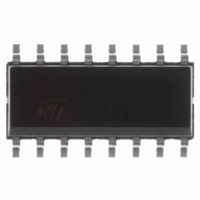
M41ST84WMQ6F STMicroelectronics, M41ST84WMQ6F Datasheet - Page 14

M41ST84WMQ6F
Manufacturer Part Number
M41ST84WMQ6F
Description
IC RTC 3V 512BIT NVRAM 16SOIC
Manufacturer
STMicroelectronics
Type
Clock/Calendar/Supervisorr
Datasheet
1.M41ST84WMQ6F.pdf
(36 pages)
Specifications of M41ST84WMQ6F
Memory Size
64B
Time Format
HH:MM:SS:hh (24 hr)
Date Format
YY-MM-DD-dd
Interface
I²C, 2-Wire Serial
Voltage - Supply
2.7 V ~ 3.6 V
Operating Temperature
-40°C ~ 85°C
Mounting Type
Surface Mount
Package / Case
16-SOIC (3.9mm Width)
Lead Free Status / RoHS Status
Lead free / RoHS Compliant
Other names
497-4693-2
Available stocks
Company
Part Number
Manufacturer
Quantity
Price
Part Number:
M41ST84WMQ6F
Manufacturer:
ST
Quantity:
20 000
Operating modes
2.2
Note:
14/36
READ mode
In this mode the master reads the M41ST84W slave after setting the slave address (see
Figure
word address ‘An’ is written to the on-chip address pointer. Next the START condition and
slave address are repeated followed by the READ mode control bit (R/W = 1). At this point
the master transmitter becomes the master receiver. The data byte which was addressed
will be transmitted and the master receiver will send an acknowledge bit to the slave
transmitter. The address pointer is only incremented on reception of an acknowledge clock.
The M41ST84W slave transmitter will now place the data byte at address An+1 on the bus,
the master receiver reads and acknowledges the new byte and the address pointer is
incremented to “An+2.”
This cycle of reading consecutive addresses will continue until the master receiver sends a
STOP condition to the slave transmitter (see
The system-to-user transfer of clock data will be halted whenever the address being read is
a clock address (00h to 07h). The update will resume either due to a stop condition or when
the pointer increments to a non-clock or RAM address.
This is true both in READ mode and WRITE mode.
An alternate READ mode may also be implemented whereby the master reads the
M41ST84W slave without first writing to the (volatile) address pointer. The first address that
is read is the last one stored in the pointer (see
Figure 8.
8). Following the WRITE mode control bit (R/W = 0) and the acknowledge bit, the
START
Slave address location
1
Doc ID 7530 Rev 9
1
SLAVE ADDRESS
0
1
Figure 9 on page
0
Figure 10 on page
0
0
R/W
A
15).
15).
M41ST84W
AI00602


