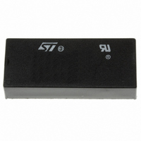
M48T512Y-70PM1 STMicroelectronics, M48T512Y-70PM1 Datasheet

M48T512Y-70PM1
Specifications of M48T512Y-70PM1
Available stocks
Related parts for M48T512Y-70PM1
M48T512Y-70PM1 Summary of contents
Page 1
... INDUSTRY STANDARD 512K X 8 SRAMS SELF-CONTAINED BATTERY and CRYSTAL in DIP PACKAGE DESCRIPTION The M48T512Y/V TIMEKEEPER RAM is a 512Kb x 8 non-volatile static RAM and real time clock or- ganized as 524,288 words by 8 bits. The special DIP package provides a fully integrated battery back-up memory and real time clock solution. ...
Page 2
... A10 formation can be accessed by the user in the 22 E same manner as any other location in the static 21 DQ7 memory array. The M48T512Y/V also has its own 20 DQ6 Power-Fail Detect circuit. This control circuitry 19 DQ5 constantly monitors the supply voltage for an out of tolerance condition. When V ...
Page 3
... Output Data Hold Time (t will go indeterminate until the next Address Ac- cess. WRITE MODE The M48T512Y the Write Mode whenever W (Write Enable) and E (Chip Enable) are low state after the address inputs are stable. The start of a write is referenced from the latter occurring falling edge ...
Page 4
... the internal battery, preserving data and pow- ering the clock. The internal energy source will maintain data in the M48T512Y/V for an accumu- lated period of at least 10 years at room tempera- ture. As system power rises above V battery is disconnected, and the power supply is ...
Page 5
... MHz) A Symbol Parameter C Input Capacitance IN (2) Input / Output Capacitance C IO Note: 1. Effective capacitance measured with power supply at 5V (M48T512Y) or 3.3V (M48T512V). Sampled only, not 100% tested. 2. Outputs deselected. Table 6A. DC Characteristics ( ° 4.5V to 5.5V Symbol Parameter (1) Input Leakage Current ...
Page 6
... M48T512Y, M48T512V Figure 5. Power Down/Up Mode AC Waveforms PFD (max) V PFD (min tWP INPUTS RECOGNIZED (Including E) OUTPUTS VALID Table 7. Power Down/Up Trip Points DC Characteristics ( °C) A Symbol V Power-fail Deselect Voltage PFD V Battery Back-up Switchover Voltage SO (2) Expected Data Retention Time t DR Note: 1. All voltages referenced 25° ...
Page 7
... Bit D7 within 7FFF9h. Setting '1' stops the oscillator. The M48T512Y/V is shipped from STMicroelectronics with the STOP bit set to a '1'. When reset to a '0', the M48T512Y/V oscillator starts after approximately one second. Note not necessary to set the WRITE bit when setting or resetting the FREQUENCY TEST bit (FT) or the STOP bit (ST) ...
Page 8
... Note 5pF goes low simultaneously with W going low, the outputs remain in the high impedance state. Calibrating the Clock. The M48T512Y/V is driv quartz controlled oscillator with a nominal frequency of 32,768Hz. The devices are factory calibrated at 25°C and tested for accuracy. Clock accuracy will not exceed 35 ppm (parts per million) oscillator frequency error at 25° ...
Page 9
... E G DQ0-DQ7 Figure 8. Write Enable Controlled, Write AC Waveforms A0-A18 E W DQ0-DQ7 tAVAV VALID tAVQV tELQV tELQX tGLQV tGLQX tAVAV VALID tAVWH tAVEL tWLWH tAVWL tWLQZ tDVWH M48T512Y, M48T512V tAXQX tEHQZ tGHQZ DATA OUT AI02389 tWHAX tWHQX tWHDX DATA INPUT AI02386 9/14 ...
Page 10
... Figure 10 il- lustrates a TIMEKEEPER calibration waveform. One method for ascertaining how much calibration a given M48T512Y/V may require involves setting the clock, letting it run for a month and comparing known accurate reference and recording de- viation over a fixed period of time. ...
Page 11
... Figure 10. Calibration Waveform NORMAL POSITIVE CALIBRATION NEGATIVE CALIBRATION Data Year Month 10 Date Date Hours Hours Minutes Seconds Calibration M48T512Y, M48T512V Function/Range BCD Format D1 D0 Year Month Date Day Day Hour Minutes Seconds Control 00-99 01-12 01-31 01-07 00-23 00-59 00-59 AI00594B 11/14 ...
Page 12
... M48T512Y, M48T512V Table 12. Ordering Information Scheme Example: Device Type M48T Supply Voltage and Write Protect Voltage 512Y = V = 4.5V to 5.5V 4.2V to 4.5V CC PFD 512V = V = 3.0V to 3.6V 2.7V to 3.0V CC PFD Speed -70 = 70ns - Package PM = PMDIP32 Temperature Range °C For a list of available options (Speed, Package, etc...) or for further information on any aspect of this de- vice, please contact the ST Sales Office nearest to you ...
Page 13
... M48T512Y, M48T512V inches Typ Min Max 0.365 0.375 0.015 0.017 0.023 0.008 0.013 1.670 1.700 0.710 0.740 0.090 0.110 1.350 1.650 0.590 0.630 0.120 0.150 0.075 ...
Page 14
... M48T512Y, M48T512V Information furnished is believed to be accurate and reliable. However, STMicroelectronics assumes no responsibility for the consequences of use of such information nor for any infringement of patents or other rights of third parties which may result from its use. No license is granted by implication or otherwise under any patent or patent rights of STMicroelectronics. Specifications mentioned in this publication are subject to change without notice ...


