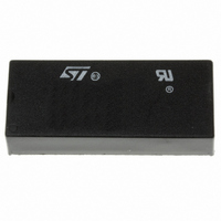
M48T512Y-70PM1 STMicroelectronics, M48T512Y-70PM1 Datasheet - Page 4

M48T512Y-70PM1
Manufacturer Part Number
M48T512Y-70PM1
Description
IC TIMEKPR NVRAM 4MBIT 5V 32-DIP
Manufacturer
STMicroelectronics
Series
Timekeeper®r
Type
Clock/Calendar/NVSRAMr
Specifications of M48T512Y-70PM1
Memory Size
4M (512K x 8)
Time Format
HH:MM:SS (24 hr)
Date Format
YY-MM-DD-dd
Interface
Parallel
Voltage - Supply
4.5 V ~ 5.5 V
Operating Temperature
0°C ~ 70°C
Mounting Type
Through Hole
Package / Case
32-DIP (600 mil) Module
Clock Format
BCD
Clock Ic Type
Timekeeper
Memory Configuration
512K X 8
Supply Voltage Range
4.5V To 5.5V
Digital Ic Case Style
DIP
No. Of Pins
32
Operating Temperature Range
0°C To +70°C
Rohs Compliant
Yes
Nvram Features
RTC, Internal Battery, XTAL
Access Time
70ns
Memory Case Style
DIP
Bus Type
Parallel
User Ram
512KB
Operating Supply Voltage (typ)
5V
Operating Supply Voltage (max)
5.5V
Operating Supply Voltage (min)
4.5V
Operating Temperature Classification
Commercial
Operating Temperature (max)
70C
Operating Temperature (min)
0C
Pin Count
32
Mounting
Through Hole
Lead Free Status / RoHS Status
Contains lead / RoHS non-compliant
Other names
497-2856-5
Available stocks
Company
Part Number
Manufacturer
Quantity
Price
Company:
Part Number:
M48T512Y-70PM1
Manufacturer:
NIPPON
Quantity:
34 000
M48T512Y, M48T512V
Figure 4. Block Diagram
DATA RETENTION MODE
With valid V
as a conventional BYTEWIDE™ static RAM.
Should the supply voltage decay, the RAM will au-
tomatically deselect, write protecting itself when
V
dow. All outputs become high impedance and all
inputs are treated as "don't care".
Note: A power failure during a write cycle may cor-
rupt data at the current addressed location, but
does not jeopardize the rest of the RAM's content.
At voltages below V
in a write protected state, provided the V
time is not less than t
spond to transient noise spikes on V
into the deselect window during the time the de-
vice is sampling V
power supply lines is recommended. When V
drops below V
er to the internal battery, preserving data and pow-
ering the clock. The internal energy source will
maintain data in the M48T512Y/V for an accumu-
lated period of at least 10 years at room tempera-
ture. As system power rises above V
battery is disconnected, and the power supply is
4/14
CC
falls between V
32,768 Hz
CRYSTAL
LITHIUM
CELL
CC
SO
applied, the M48T512Y/V operates
, the control circuit switches pow-
CC
PFD
.Therefore, decoupling of the
PFD
F
. The M48T512Y/V may re-
(min), the memory will be
(max), V
OSCILLATOR AND
VOLTAGE SENSE
CLOCK CHAIN
SWITCHING
CIRCUITRY
AND
V CC
PFD
CC
(min) win-
that cross
SO
CC
, the
POWER
fall
CC
V PFD
switched to external V
ues until V
Normal RAM operation can resume t
exceeds V
(AN1012) on the ST Web Site for more information
on battery life.
CLOCK OPERATIONS
Reading the Clock Updates to the TIMEKEEPER
registers should be halted before clock data is
read to prevent reading data in transition. Because
the BiPORT TIMEKEEPER cells in the RAM array
are only data registers, and not the actual clock
counters, updating the registers can be halted
without disturbing the clock itself. Updating is halt-
ed when a '1' is written to the READ bit, D6 in the
Control Register (7FFF8h). As long as a '1' re-
mains in that position, updating is halted. After a
halt is issued, the registers reflect the count; that
is, the day, date, and time that were current at the
moment the halt command was issued. All of the
TIMEKEEPER registers are updated simulta-
neously. A halt will not interrupt an update in
progress. Updating occurs 1 second after the
READ bit is reset to a '0'.
SRAM ARRAY
TIMEKEEPER
524,280 x 8
REGISTERS
CC
PFD
8 x 8
V SS
reaches V
(max). Refer to Application Note
CC
PFD
. Write protection contin-
(min) plus t
A0-A18
DQ0-DQ7
E
W
G
ER
AI02384
after V
ER
(min).
CC


