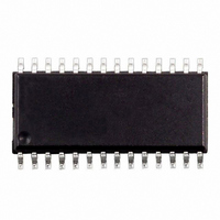
M41ST85WMX6 STMicroelectronics, M41ST85WMX6 Datasheet - Page 26

M41ST85WMX6
Manufacturer Part Number
M41ST85WMX6
Description
IC RTC 3.0V NVRAM 28SOIC
Manufacturer
STMicroelectronics
Type
Clock/Calendar/Supervisorr
Specifications of M41ST85WMX6
Memory Size
64B
Time Format
HH:MM:SS:hh (24 hr)
Date Format
YY-MM-DD-dd
Interface
I²C, 2-Wire Serial
Voltage - Supply
2.7 V ~ 3.6 V
Operating Temperature
-40°C ~ 85°C
Mounting Type
Surface Mount
Package / Case
28-SOIC, 28-SOH (8.48mm Width)
Function
Clock/Calendar/Supervisor/Alarm
Rtc Memory Size
64 Byte
Supply Voltage (max)
3.6 V
Supply Voltage (min)
2.7 V
Maximum Operating Temperature
+ 85 C
Minimum Operating Temperature
- 40 C
Mounting Style
SMD/SMT
Rtc Bus Interface
Serial (2-Wire, I2C)
Memory Configuration
64 X 8
Nvram Features
RTC, Internal Battery, XTAL
Interface Type
I2C, Serial, 2-Wire
Supply Voltage Range
2.7V To 3.6V
Memory Case Style
SO
No. Of Pins
28
Rohs Compliant
Yes
Lead Free Status / RoHS Status
Lead free / RoHS Compliant
Other names
497-2805-5
Available stocks
Company
Part Number
Manufacturer
Quantity
Price
Part Number:
M41ST85WMX6
Manufacturer:
ST
Quantity:
20 000
Part Number:
M41ST85WMX6TR
Manufacturer:
ST
Quantity:
20 000
Clock operation
3.8
Figure 17. RSTIN1 & RSTIN2 timing waveforms
Note:
Table 5.
1. Valid for ambient operating temperature: T
2. Pulse width less than 50 ns will result in no RESET (for noise immunity).
3. Pulse width less than 20 ms will result in no RESET (for noise immunity).
4. Programmable (see
3.9
26/41
t
t
t
t
Symbol
R1HRH
R2HRH
RLRH1
RLRH2
RSTIN1
RSTIN2
RST
(2)
(3)
(4)
(4)
Reset inputs (RSTIN1 & RSTIN2)
The M41ST85W provides two independent inputs which can generate an output reset. The
duration and function of these resets is identical to a reset generated by a power cycle.
Table 5
than t
internally pulled up to V
With pull-up resistor
Reset AC characteristics
Power-fail input/output
The power-fail input (PFI) is compared to an internal reference voltage (1.25 V). If PFI is less
than the power-fail threshold (V
intended for use as an undervoltage detector to signal a failing power supply. Typically PFI is
connected through an external voltage divider (see
unregulated DC input (if it is available) or the regulated output of the V
voltage divider can be set up such that the voltage at PFI falls below V
milliseconds before the regulated V
below the minimum operating voltage.
During battery backup, the power-fail comparator turns off and PFO goes (or remains) low.
This occurs after V
irrespective of V
inputs are recognized. At the end of this time, the power-fail comparator is enabled and PFO
(1)
RLRH1
Table 6 on page
RSTIN1 low to RSTIN1 high
RSTIN2 low to RSTIN2 high
RSTIN1 high to RST high
RSTIN2 high to RST high
and
Figure 17
and t
PFI
RLRH2
CC
for the write protect time (t
Parameter
28).
drops below V
illustrate the AC reset characteristics of this function. Pulses shorter
tRLRH1
CC
will not generate a reset condition. RSTIN1 and RSTIN2 are each
A
= –40 to 85°C; V
tR1HRH
through a 100 k
(1)
PFI
), the power-fail output (PFO) will go low. This function is
CC
PFD
tRLRH2
input to the M41ST85W or the microprocessor drops
CC
(min). When power returns, PFO is forced high,
= 2.7 to 3.6 V (except where noted).
resistor.
rec
), which is the time from V
Min
200
100
Figure 5 on page
40
40
tR2HRH
Max
200
200
11) to either the
CC
PFI
regulator. The
PFD
several
AI03665
(max) until the
M41ST85W
Unit
ms
ms
ms
ns


