DP8573AVX/NOPB National Semiconductor, DP8573AVX/NOPB Datasheet - Page 14
DP8573AVX/NOPB
Manufacturer Part Number
DP8573AVX/NOPB
Description
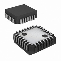
IC REAL TIME CLOCK (RTC) 28-PLCC
Manufacturer
National Semiconductor
Type
Clock/Calendar/NVSRAMr
Datasheet
1.DP8573AVXNOPB.pdf
(16 pages)
Specifications of DP8573AVX/NOPB
Memory Size
32B
Time Format
HH:MM:SS:hh (12/24 hr)
Date Format
YY-MM-DD-dd
Interface
Parallel
Voltage - Supply
4.5 V ~ 5.5 V
Operating Temperature
-40°C ~ 85°C
Mounting Type
Surface Mount
Package / Case
28-PLCC
Bus Type
Parallel
Operating Supply Voltage (typ)
5V
Package Type
PLCC
Operating Supply Voltage (max)
5.5V
Operating Supply Voltage (min)
4.5V
Operating Temperature Classification
Industrial
Operating Temperature (max)
85C
Operating Temperature (min)
-40C
Pin Count
28
Mounting
Surface Mount
Lead Free Status / RoHS Status
Lead free / RoHS Compliant
Other names
*DP8573AVX
*DP8573AVX/NOPB
DP8573AVX
*DP8573AVX/NOPB
DP8573AVX
Available stocks
Company
Part Number
Manufacturer
Quantity
Price
Company:

Part Number:
DP8573AVX/NOPB
Manufacturer:
Texas Instruments
Quantity:
10 000


Application Hints
5
6
Typical Application
Test bit D6 in the Periodic Flag Register
IF a 1 go to 4 1 If this bit remains a 1 after 3 seconds
then abort and check hardware The crystal may be de-
fective or not installed There may be a short at OSC IN
or OSC OUT to V
is less than 10 M
IF a 0 then the oscillator is running go to step 7
Write a 0 to bit D6 in the Periodic Flag Register This
action puts the clock chip in the battery backed mode
This mode can be entered only if the OSC fail flag (bit
D6 of the Periodic Flag Register) is a 0 Reminder bit D6
is a dual function bit When read D6 returns oscillator
status When written D6 causes either the Battery
Backed Mode or the Single Supply Mode of operation
CC
or GND or to some impedance that
(Continued)
These components may be necessary to meet UL requirements
for lithium batteries Consult battery manufacturer
14
7
8
9
The only method to ensure the chip is in the battery
backed mode is to measure the waveform at the OSC
OUT pin If the battery backed mode was selected suc-
cessfully then the peak to peak waveform at OSC OUT
is referenced to the battery voltage If not in battery
backed mode the waveform is referenced to V
measurement should be made with a high impedance
low capacitance probe (10 M
probe or better) Typical peak to peak swings are within
0 6V of V
Write a 1 to bit D7 of Interrupt Control Register 1 This
action enables the PFAIL pin and associated circuitry
Write a 1 to bit D4 of the Real Time Mode Register This
action ensures that bit D7 of Interrupt Control Register 1
remains a 1 when V
Initialize the rest of the chip as needed
CC
and ground respectively
BB l
V
CC
(Standby Mode)
10 pF oscilloscope
TL F 9981– 19
CC
The
Related parts for DP8573AVX/NOPB
Image
Part Number
Description
Manufacturer
Datasheet
Request
R

Part Number:
Description:
IC REAL TIME CLOCK (RTC) 28-PLCC
Manufacturer:
National Semiconductor
Datasheet:

Part Number:
Description:
Clock IC
Manufacturer:
National Semiconductor
Datasheet:

Part Number:
Description:
National Semiconductor [8-Bit D/A Converter]
Manufacturer:
National Semiconductor
Datasheet:
Part Number:
Description:
National Semiconductor [Media Coprocessor]
Manufacturer:
National Semiconductor
Datasheet:
Part Number:
Description:
Digitally Controlled Tone and Volume Circuit with Stereo Audio Power Amplifier, Microphone Preamp Stage and National 3D Sound
Manufacturer:
National Semiconductor
Datasheet:
Part Number:
Description:
Digitally Controlled Tone and Volume Circuit with Stereo Audio Power Amplifier, Microphone Preamp Stage and National 3D Sound
Manufacturer:
National Semiconductor
Datasheet:
Part Number:
Description:
AC97 Rev 2 Codec with Sample Rate Conversion and National 3D Sound
Manufacturer:
National Semiconductor
Part Number:
Description:
Manufacturer:
National Semiconductor
Datasheet:
Part Number:
Description:
Manufacturer:
National Semiconductor
Datasheet:
Part Number:
Description:
General Purpose, Low Voltage, Low Power, Rail-to-Rail Output Operational Amplifiers
Manufacturer:
National Semiconductor
Datasheet:
Part Number:
Description:
8-bit 20 MSPS flash A/D converter.
Manufacturer:
National Semiconductor
Datasheet:
Part Number:
Description:
Low Noise Quad Operational Amplifier
Manufacturer:
National Semiconductor
Datasheet:
Part Number:
Description:
Quad Differential Line Receivers
Manufacturer:
National Semiconductor
Datasheet: